diff options
Diffstat (limited to '_posts/featured')
| -rw-r--r-- | _posts/featured/2020-10-24-tiny-linux-c-binaries.md | 388 | ||||
| -rw-r--r-- | _posts/featured/2024-03-20-rf-primer.md | 753 |
2 files changed, 1141 insertions, 0 deletions
diff --git a/_posts/featured/2020-10-24-tiny-linux-c-binaries.md b/_posts/featured/2020-10-24-tiny-linux-c-binaries.md new file mode 100644 index 0000000..1966d45 --- /dev/null +++ b/_posts/featured/2020-10-24-tiny-linux-c-binaries.md @@ -0,0 +1,388 @@ +--- +layout: post +date: 2020-10-24 +title: Tiny C Binaries +author: Dylan Müller +--- + +> By default, following the linking stage, `GCC` generates `ELF` binaries that contain +> redundant section data that increase executable size. + +1. [ELF Binaries](#elf-binaries) +2. [Size Optimisation](#size-optimisation) +3. [Linux Syscalls](#linux-syscalls) +4. [Custom Linker Script](#custom-linker-script) +5. [GCC flags](#gcc-flags) +6. [SSTRIP](#sstrip) +7. [Source Code](#source-code) + +# ELF Binaries + +The standard file format for executable object code on Linux is `ELF` (Executable +and Linkable Format), it is the successor to the older `COFF` `UNIX` file format. + +`ELF` Binaries consist of two sections, the `ELF` header and file data (object +code). The `ELF` header format for `64-bit` binaries is shown in the table below: + +| Offset | Field | Description | Value | +|--------|------------------------|----------------------------------------|---------------------------------------------------------------------------------------| +| 0x00 | e_ident[EI_MAG0] | magic number | 0x7F | +| 0x04 | e_ident[EI_CLASS] | 32/64-bit | 0x2 = 64-bit | +| 0x05 | e_ident[EI_DATA] | endianness | 0x1 = little<br>0x2 = big | +| 0x06 | e_ident[EI_VERSION] | elf version | 0x1 = original | +| 0x07 | e_ident[EI_OSABI] | system ABI | 0x00 = System V<br>0x02 = NetBSD<br>0x03 = Linux<br>0x09 = FreeBSD<br> | +| 0x08 | e_ident[EI_ABIVERSION] | ABI Version | * ignored for static-linked binaries<br>* vendor specific for dynamic-linked binaries | +| 0x09 | e_ident[EI_PAD] | undefined | * padded with zeros | +| 0x10 | e_type | object type | 0x00 = ET_NONE<br>0x01 = ET_REL<br>0x02 = ET_EXEC<br>0x03 = ET_DYN<br>0x04 = ET_CORE | +| 0x12 | e_machine | system ISA | 0x3E = amd64<br>0xB7 = ARM (v8/64) | +| 0x14 | e_version | elf version | 0x1 = original | +| 0x18 | e_entry | entry point | 64-bit entry point address | +| 0x20 | e_phoff | header table offset | 64-bit program header table offset | +| 0x28 | e_shoff | section table offset | 64-bit section header table offset | +| 0x30 | e_flags | undefined | vendor specific or pad with zeros | +| 0x34 | e_ehsize | elf header size | 0x40 = 64bits, 0x20 = 32bits | +| 0x36 | e_phentsize | header table size | - | +| 0x38 | e_phnum | #(num) entries in header table | - | +| 0x3A | e_shentsize | section table size | - | +| 0x3C | e_shnum | #(num) entries in section table | - | +| 0x3E | e_shstrndx | section names index into section table | - | +| 0x40 | | | End of 64-bit ELF | + +These data fields are used by the Linux `PL` (program loader) to resolve the entry +point for code execution along with various fields such as the `ABI` version, `ISA` +type, as well as section listings. + +A sample hello world program is shown below and was compiled with `GCC` using `gcc +main.c -o example`. + +``` +#include <stdio.h> + +int main(int agrc, char *argv[]){ + printf("Hello, World!"); + return 0; +} +``` + +This produced an output executable of almost **~17 KB** ! If you've ever +programmed in assembly you might be surprised at the rather large file size for +such a simple program. + +`GNU-binutils` `objdump` allows us to inspect the full list of `ELF` sections with +the `-h` flag. + +After running `objdump -h example` on our sample binary we see that there are a +large number of `GCC` derived sections: `.gnu.version` and `.note.gnu.property` +attached to the binary image. The question becomes how much data these +additional sections are consuming and to what degree can we 'strip' out +redundant data. + +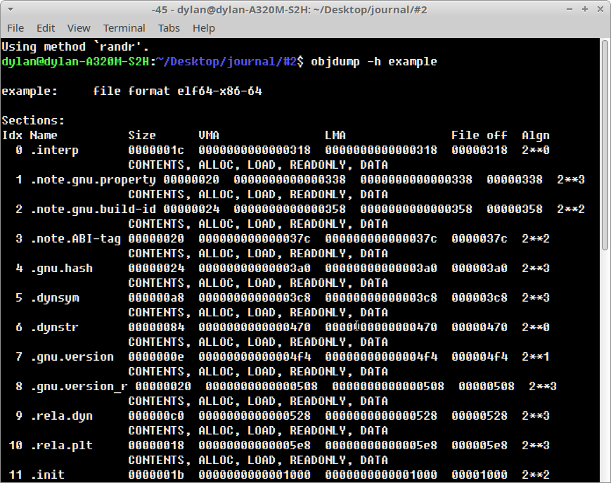 + +`GNU-binutils` comes with a handy utility called `strip`, which attempts to remove +unused `ELF` sections from a binary. Running `strip -s example` results only in a +slightly reduced file of around **~14.5 KB**. Clearly, we need to strip much +more! :open_mouth: + +# Size Optimisation + +`GCC` contains a large number of optimisation flags, these include the common : +`-O2 -O3 -Os` flags as well as many more less widely used compile time options, +which we will explore further. However, since we have not yet compiled with any +optimisation thus far, and as a first step we recompile the above example with +`-Os`, to optimise for size. + + + +And we see no decrease in size! This is expected behaviour however, since the +`-Os` flag does not consider all redundant section data for removal, on the +contrary the additional section information placed by `GCC` in the output binary +is considered useful at this level of optimisation. + +In addition, the use of `printf` binds object code from the standard library +into the final output executable and so we will instead call through to the +Linux kernel directly to print to the standard output stream. + +# Linux syscalls + +System calls on Linux are invoked with the `x86_64` `syscall` opcode and syscall +parameters follow a very specific order on `64-bit` architectures. For `x86_64` +([System V ABI - Section +A.2.1](https://refspecs.linuxfoundation.org/elf/x86_64-abi-0.99.pdf)), the order +of parameters for linux system calls is as follows: + +| description | register (64-bit) | +|----------------|----------| +| syscall number | rax | +| arg 1 | rdi | +| arg 2 | rsi | +| arg 3 | rdx | +| arg 4 | r10 | +| arg 5 | r8 | +| arg 6 | r9 | + + +Arguments at user mode level (`__cdecl` calling convention), however, are parsed in +the following order: + +| description | register (64-bit) | +|-------------|-----| +| arg 1 | rdi | +| arg 2 | rsi | +| arg 3 | rdx | +| arg 4 | rcx | +| arg 5 | r8 | +| arg 6 | r9 | + +To call through to the linux kernel from `C`, an assembly wrapper was required to +translate user mode arguments (`C` formal parameters) into kernel `syscall` +arguments: + +``` +syscall: + mov rax,rdi + mov rdi,rsi + mov rsi,rdx + mov rdx,rcx + mov r10,r8 + mov r8,r9 + syscall + ret +``` + +We may then make a call to this assembly routine from `C` using the following +function signature: + +``` +void* syscall( + void* syscall_number, + void* param1, + void* param2, + void* param3, + void* param4, + void* param5 +); +``` + +To write to the standard output stream we invoke syscall `0x1`, which handles +file output. A useful `x86_64` Linux syscall table can be found +[here](https://blog.rchapman.org/posts/Linux_System_Call_Table_for_x86_64/). +Syscall `0x1` takes three arguments and has the following signature: + +`sys_write( unsigned int fd, const char *buf, size_t count)` + +A file called `base.c` was created, implementing both `syscall` and print wrappers: + +``` +// base.c +typedef unsigned long int uintptr; +typedef long int intptr; + +void* syscall( + void* syscall_number, + void* param1, + void* param2, + void* param3, + void* param4, + void* param5 +); + +static intptr print(void const* data, uintptr nbytes) +{ + return (intptr) + syscall( + (void*)1, /* sys_write */ + (void*)(intptr)1, /* STD_OUT */ + (void*)data, + (void*)nbytes, + 0, + 0 + ); +} + +int main(int agrc, char *argv[]){ + print("Hello, World", 12) + return 0; +} +``` + +In order to instruct `GCC` to prevent linking in standard library object code, the +`-nostdlib` flag should be passed at compile time. There is one caveat however, +in that certain symbols, such as `_start` , which handle program startup and the +parsing of the command line arguments to `main` , will be left up to us to +implement, otherwise we will segfault :-/ + +However, this is quite trivial and luckily program initialisation is well +defined by -- [System V ABI - Section +3.4](https://refspecs.linuxfoundation.org/elf/x86_64-abi-0.99.pdf). + +Initially it is specified that register `rsp` hold the argument count, while the +address given by `rsp+0x8` hold an array of `64-bit` pointers to the argument +strings. + +From here the argument count and string pointer array index can be passed to +`rdi` and `rsi` respectively, the first two parameters of `main()` . Upon exit, +a call to syscall `0x3c` is then made to handle program termination gracefully. + +Both the syscall and program startup assembly wrappers (written in GAS) were +placed in a file called `boot.s`: + +``` +/* boot.s */ +.intel_syntax noprefix +.text +.globl _start, syscall + +_start: + xor rbp,rbp /* rbp = 0 */ + pop rdi /* rdi = argc, rsp= rsp + 8 */ + mov rsi,rsp /* rsi = char *ptr[] */ + and rsp,-16 /* align rsp to 16 bytes */ + call main + mov rdi,rax /* rax = main return value */ + mov rax,60 /* syscall= 0x3c (exit) */ + syscall + ret + +syscall: + mov rax,rdi + mov rdi,rsi + mov rsi,rdx + mov rdx,rcx + mov r10,r8 + mov r8,r9 + syscall + ret +``` + +Finally gcc was invoked with `gcc base.c boot.s -nostdlib -o base`. + +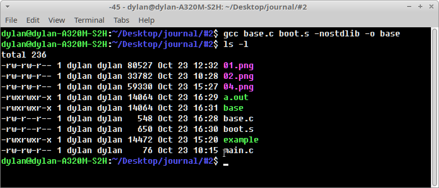 + +Wait what!? We still get a **~14 KB** executable after all that work? Yep, and +although we have optimised the main object code for our example, we have not yet +stripped out redundant `ELF` code sections which contribute a majority of the file +size. + +# Custom Linker Script + +Although it is possible to strip some redundant sections from an `ELF` binary +using `strip`, it is much more efficient to use a custom linker script. + +A linker script specifies precisely which `ELF` sections to include in the output +binary, which means we can eliminate *almost* all redundancy. Care, however, +must be taken to ensure that essential segments such as `.text`, `.data`, +`.rodata*` are not discarded during linking to avoid a segmentation fault. + +The linker script that I came up with is shown below (`x86_64.ld`): + +``` +OUTPUT_FORMAT("elf64-x86-64", "elf64-x86-64", + "elf64-x86-64") +OUTPUT_ARCH(i386:x86-64) +ENTRY(_start) + +SECTIONS +{ + . = 0x400000 + SIZEOF_HEADERS; + .text : { *(.text) *(.data*) *(.rodata*) *(.bss*) } +} +``` + +The linker script sets the virtual base address of the output binary to `0x400000` +and retains only the essential code segments. + +Custom linker scripts are parsed to `GCC` with the `-T` switch and the resulting +binary was compiled with: `gcc -T x86_64.ld base.c boot.s -nostdlib -o base`. + +This produced an output executable of around **~2.7 KB**. + +This is much better, but there is still some room for improvement using +additional `GCC` compile time switches. + +# GCC Flags + +We have thus far managed to shrink our executable size down to **~2.7 KB** from our +initial file size of **~17 KB** by stripping redundant section data using a custom +linker script and removing standard library object code. + +However, `GCC` has several compile time flags that can further help in removing +unwanted code sections, these include: + +| flag | description | +|----------------------|---------------------------------------| +| -ffunction-sections | place each function into own section | +| -fdata-sections | place each data item into own section | +| -Wl,\--gc-sections | strip unused sections (linker) | +| -fno-unwind-tables | remove unwind tables | +| -Wl,\--build-id=none | remove build-id section | +| -Qn | remove .ident directives | +| -Os | optimize code for size | +| -s | strip all sections | + +Compiling our example again with: `gcc -T x86_64.ld base.c boot.s -nostdlib -o +base -ffunction-sections -fdata-sections -Wl,--gc-sections -fno-unwind-tables +-Wl,--build-id=none -Qn -Os -s`. + +This produces an output executable with a size of **~1.5 KB** but we can still go +further! + +Additionally, you can include the `-static` switch to ensure a static binary. +This results in an output executable of **~640 bytes**. + +# SSTRIP + +Despite all our optimisation thus far, there are still a few redundant code and +data sections in our dynamically linked output executable. Enter `sstrip`... + +[sstrip](https://github.com/aunali1/super-strip) is a useful utility that +attempts to identify which sections of an `ELF` binary are to be loaded into +memory during program execution. Based off this, all unused code and data +sections are then subsequently removed. It is comparable to `strip` but performs +section removal more aggressively. + +Running `./sstrip base` we get our final executable binary with a size of **~830 +bytes** ! + +At this point it would probably be best to switch to assembly to get smaller +file sizes, however the goal of this `journal` was to create small executables +written in `C` and I think we've done quite well to reduce in size from **~17 KB** +down to **~830 bytes**! + +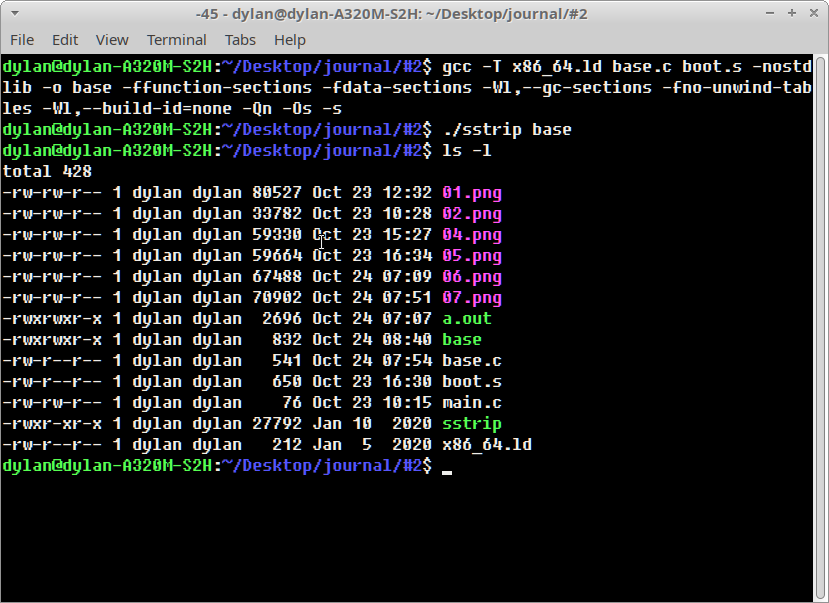 + +As a final comment you might be wondering if we could have simply run `sstrip` +from our **17 KB** executable in the first place and the answer would be, no. + +I tried doing this and ended up with a binary image of around **~12 KB** so it seems +the sstrip needs a bit of additional assistance in the form our our manual +optimisations to get really `tiny` binaries! + +# Source Code + +Source code used in this `journal` is available at: +[https://github.com/lunar-sh/tinybase](https://github.com/lunar-sh/tinybase) + +# Signature + +``` ++---------------------------------------+ +| .-. .-. .-. | +| / \ / \ / \ + | +| \ / \ / \ / | +| "_" "_" "_" | +| | +| _ _ _ _ _ _ ___ ___ _ _ | +| | | | | | | \| | /_\ | _ \ / __| || | | +| | |_| |_| | .` |/ _ \| /_\__ \ __ | | +| |____\___/|_|\_/_/ \_\_|_(_)___/_||_| | +| | +| | +| Lunar RF Labs | +| Email: root@lunar.sh | +| | +| Research Laboratories | +| OpenAlias (BTC, XMR): lunar.sh | +| Copyright (C) 2022-2024 | ++---------------------------------------+ +``` diff --git a/_posts/featured/2024-03-20-rf-primer.md b/_posts/featured/2024-03-20-rf-primer.md new file mode 100644 index 0000000..43ffcb1 --- /dev/null +++ b/_posts/featured/2024-03-20-rf-primer.md @@ -0,0 +1,753 @@ +--- +layout: post +title: RF Circuit and Power Amplifier Design Basics +date: 2024-03-20 +author: Dylan Müller +--- + +> A short primer on some of the basic concepts related to `RF` circuit +> and `RF` power amplifier design. + +1. [Average Power](#average-power) +2. [Transmission Lines](#transmission-lines) +3. [Impedance Matching](#impedance-matching) +4. [Electromagnetic Transducers](#electromagnetic-transducers) +5. [S-Parameters](#s-parameters) +6. [Harmonic Balance](#harmonic-balance) +7. [Lumped and Distributed Element Networks](#lumped-and-distributed-element-networks) +8. [Classes Of Operation](#classes-of-operation) +9. [Stability Analysis](#stability-analysis) +10. [Efficiency](#efficiency) +11. [P1dB Compression Point](#p1db-compression-point) +12. [Load Pull](#load-pull) +13. [LC Filtering](#lc-filtering) + +# Foreword + +The aim of this journal entry is to review some basic technical concepts +pertaining to general `RF` circuit design and modelling as well as `RF` power +amplifier design. + +`RF` circuit design is typically not covered in detail at an undergraduate level +and the author hopes that this journal entry will provide some useful +information to readers not familiar with the subject. + +# Average Power + +In order to be successful in `RF` power amplifier design, it is necessary to +understand `AC` power from both a frequency and time domain perspective. + +In the frequency-domain, complex `AC` power ($$S$$) is given by: + +$$ S = \overline{V}.\overline{I}^* $$ + +Where $$\overline{V}$$ and $$\overline{I}$$ are the voltage and current phasors. In +`RF` power amplifier design we are typically concerned with maximizing the real +component of complex power $$\Re(S)$$ which represents power dissipated in a load +such as an antenna (modelled by it's radiation resistance). The imaginary part +of $$S$$ represents reactive power which does not perform any useful work. + +Average real power ($$P_{avg}$$) is the industry standard measure of power for `RF` +and `microwave` systems and is measured in the `SI` units of `watts (W)`. Average +power over total time ($$T$$) for a continuous-wave (`CW`) signal is defined by the +following time-domain integral: + +$$ P_{avg} = \frac{1}{T} \int\limits_0^T v(t).i(t) dt $$ + +The terms $$v(t)$$ and $$i(t)$$ can then be expanded: + +$$ v(t) = v_{p}sin(2\pi ft), i(t) = i_{p}sin(2\pi ft + \theta) $$ + +Here $$\theta$$ represents the phase angle between $$i(t)$$ and $$v(t)$$ and ($$v_{p}$$) +and ($$i_{p}$$) represent the peak values of the voltage and current waveforms. + +It can be shown that for purely sinusoidal voltage and current waveforms: + +$$ P_{avg} = \frac{1}{2}v_{p}i_{p}cos(\theta) $$ + +Hence maximum real power is obtained when the current and voltage waveforms are +in phase. $$cos (\theta)$$ is commonly referred to as the power factor and this +constant relates real power to apparent power $$\|S\|$$. Apparent power is the +total complex power available to a particular load. + +In practice average real power is specified in terms of decibels referenced to `1` +`milliwatt (mW)` ($$dBm$$): + +$$ dBm(P) = 10\log_{10}(\frac{P}{1mW}) $$ + +While relative power is measured in decibels ($$dB$$): + +$$ dB(P) = 10\log_{10}(\frac{P}{P_{ref}}) $$ + +## Transmission Lines + +Traditional lumped circuit theory is only applicable to low frequency circuits +as it assumes that wires are lossless with negligible electrical length. +Electrical length is usually measured in terms of multiples of the wavelength +($$\lambda$$) of the highest frequency signal that is conducted over the line. + +As a rule of thumb, when the length of a wire is greater or equal to +$$\lambda/10$$, the voltage and current in the wire as a function of position +along the wire will no longer be constant with time and wave-like behaviour such +as reflection and standing waves start becoming important. In these cases +utilizing a distributed model, such as the transmission line, often becomes +necessary. + +Let $${u}$$ and $${i}$$ represent the voltage and current along the transmission line as +a function of position and time: + +$$ u = u(x,t), i = i(x,t) $$ + +Then at distance $${x+dx}$$ voltage and current can be expressed with a taylor +series expansion: + +$$ u(x + dx) = u(x,t) + \frac{\partial u}{\partial x} dx $$ + +$$ i(x + dx) = i(x,t) + \frac{\partial i}{\partial x} dx $$ + +A segment of a traditional transmission line is shown in the figure below. It +consists of a series distributed resistance $$R(x)$$, inductance $$L(x)$$ as well as +segment capacitance $$C(x)$$ and conductance $$G(x)$$. A transmission line is +thought of as a continuous series of these segments. + +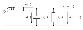 + +It can be shown that the equations that describe changes in the voltage and +current on the line is given by: + +$$ \frac{\partial u}{\partial x} dx = -Ri - L \frac{\partial i}{\partial t} $$ + +$$ \frac{\partial i}{\partial x} dx = -Gu - C \frac{\partial u}{\partial t} $$ + +The equations above are known as the telegrapher's equations. These two +equations can be combined to produce two partial differential equations with one +isolated variable each ($${u}$$ or $${i}$$). + +$$u$$ and $$i$$ are related by the characteristic impedance ($$Z_{0}$$) of the +transmission line which can be derived from the telegraphers equations: + +$$ Z_{0} = \frac{V^+(x)}{I^+(x)} = \sqrt{\frac{R(x)+j\omega L(x)}{G(x)+j\omega +C(x)}} $$ + +For most transmission lines dielectric and conductor losses are low, so we +assume: + +$$ R(x) \ll j\omega L(x), G(x) \ll j\omega C(x) $$ + +As a result the equation above simplifies to: + +$$ Z_{0} = \sqrt{\frac{L(x)}{C(x)}} $$ + +It is worth noting that characteristic impedance $$Z_{0}$$ of a transmission line +only has an effect at `RF` frequencies. It is not possible to measure the +characteristic impedance of a transmission line directly with a multimeter +because resistance (ohms law) and characteristic impedance (electromagnetic +property) are not the same concept. + +Examples of transmission lines include coaxial cable and microstrip line. +Transmission lines typically have a characteristic impedance of `50` $$\Omega$$ in +`RF` systems and are used to carry `RF` signals from one point in a circuit to +another with minimal losses. + +# Impedance Matching + +It is often said that impedance matching is what truly differentiates `RF` circuit +design from low frequency circuit design. Indeed, it is one of the most common +tasks for an `RF` designer. + +`RF` signals travelling along a transmission line can be thought of as +electromagnetic power waves. Power waves are a hypothetical construct, one of +the many possible linear transformations of voltage and current. + +The figure below shows a typical `RF circuit` consisting of a `RF` power source +($$G$$) with an impedance of ($$Z_{R}$$) and a load with an impedance of $$Z_{L}$$. +The interface of the generator and load impedance is indicated by the dotted +line. + +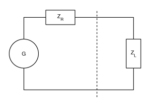 + +It is at this interface that we experience reflection of the power wave (back to +the generator) when $$Z_{R} \neq Z_{L}$$. If the impedance of the generator and +load were equal then no reflection occurs. + +In general, the goal of an `RF` system is to transfer `RF` power as efficiently from +one point to another with minimal reflections. The degree of an electromagnetic +power wave reflected (at the boundary) is determined by the reflection +coefficient ($$\Gamma$$): + +$$ \Gamma_{L} = \frac{Z_{L} - Z_{0}}{Z_{L}+Z_{0}} $$ + +A $$\Gamma$$ of $$0$$ indicates no reflection, while a $$\Gamma$$ of `1` or `-1` +represents total reflection with or without phase inversion. + +Here ($$Z_{0}$$) represents the reference impedance of the system which is +typically `50` $$\Omega$$. Maximum power transfer over the boundary from the +generator to the load is only satisfied when: + +$$ Z_{L} = Z_{R}^* $$ + +This expression is known as the conjugate match rule for maximum power transfer. +In most practical `RF` systems $$Z_{L} \neq Z_{R}$$ and so a method of impedance +transformation is required to satisfy the conjugate match rule. + +Impedance transformation networks allow a $$Z_{L}$$ with both a real and imaginary +part to be transformed into another complex impedance using reactive components. +Reactive components do not dissipate real power unlike resistors which is why +resistors are rarely used in `RF` impedance matching and filter networks. + +The most basic type of impedance transformation network is known as the `LC` +network which consists of an inductor and capacitor. It can be used to transform +a complex load ($$R_{L}$$) to `50` $$\Omega$$. The figure below shows the basic +configuration of the `LC` impedance transformation network. + +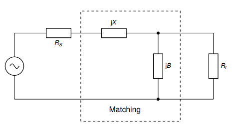 + +In addition to the `LC` network's impedance transformation property, the `LC` +network can have a low-pass or high-pass response depending on the shunt element +($$jB$$). If it is capacitive then the `LC` network will have a low-pass response or +a high-pass response if it is inductive. + +Typically the low pass configuration (with a shunt capacitor) is desired. + +It should be noted that the shunt element ($$jB$$) should be placed on the side +with the largest impedance. Therefore there are two possible configurations of +this network: + +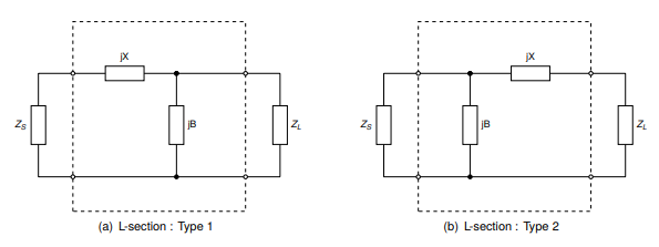 + +So that type `1` is used when $$R_{L} > R_{S}$$ and type `2` is used when $$R_{L} < +R_{S}$$. Here $$Z_{S}$$ represents $$Z_{0}$$ the system reference impedance $$(50 +\Omega)$$. + +The design procedure for a type `1` `LC` network is as follows. First we evaluate +the input impedance ($$Z_{in}$$) looking into the matching network. + +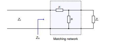 + +We start by defining a few variables. Let: + +$$ Z_{L} = R_{L} + jX_{L} $$ + +$$ Z_{S} = Z_{0} = 50 \Omega $$ + +$$ Z_{in} = jX + \frac{1}{(jB)^{-1} + (Z_{L})^{-1}} $$ + +Matching conditions are met when $$Z_{in} = Z_{S} = Z_{0}$$. + +The equation above can be simplified and separated into real and imaginary +parts: + +$$ B(X + X_{L}) = -(Z_{0}R_{L}-XX_{L}) $$ + +$$ B(R_{L} - Z_{0}) = Z_{0}X_{L} - R_{L}X $$ + +`B` can then be solved using the following equation: + +$$ B = -\frac{R_{L}^2+X_{L}^2}{X_{L} + \sqrt{\frac{R_{L}}{Z_{0}}} \sqrt{R_{L}^2 + X_{L}^2 - Z_{0}R_{L}}} $$ + +Once `B` is obtained, X may be found by rearranging for `X`: + +$$ X = \frac{B(R_{L} - Z_{0}) - Z_{0}X_{L}}{-R_{L}} $$ + +The figure below depicts the second variant of the `LC` matching network. + +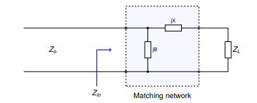 + +Let: + +$$ Z_{L} = R_{L} + jX_{L} $$ + +$$ Z_{S} = Z_{0} = 50 \Omega $$ + +$$ Z_{in} = \frac{1}{(jB)^{-1} + (Z_{L} + jX)^{-1}} $$ + +Matching conditions are met when $$Z_{in} = Z_{S} = Z_{0}$$. + +The equation above can be simplified and separated into real and imaginary +parts: + +$$ B(X_{L} + X) = -Z_{0}R_{L} $$ + +$$ B(Z_{0} - R_{L}) = -Z_{0}(X_{L}+X) $$ + +Again, B can then be solved using the following equation: + +$$ B = -Z_{0}\sqrt{\frac{R_{L}}{Z_{0}- R_{L}}} $$ + +Again, `X` may be found by rearranging for $$(X_{L} + X)$$ and substituting to +yield: + +$$ X = \sqrt{R_{L}(Z_{0} - R_{L})} - X_{L} $$ + +For both `LC` circuit types it is assumed that $$jB$$ represents a capacitive +element and $$jX$$ represents an inductive element so that a low-pass response is +obtained. + +Matching networks with more than two reactive elements also exist. These include +the $$\pi$$-section and `T-section` matching networks that contain `3` reactive +elements each. The figure below depicts the $$\pi$$-section network. + +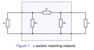 + +The $$\pi$$-section network is made up of a type `2` `LC` matching network in cascade +with a type 1 `LC` matching network. The central element $$jX$$ is the sum of the +inductive reactance ($$jX$$) of each `LC` matching section, which is combined into a +single reactance. + +A virtual load resistance $$R_{x}$$ is interposed in-between the two `LC` matching +networks. The goal of the first `LC` matching network is to then match the source +$$Z_{S}$$ to $$R_{x}$$ while the second `LC` matching network matches $$R_{x}$$ to +$$Z_{L}$$. + +The value of $$R_{x}$$ is chosen according to the desired `Q-factor` and must be +smaller than $$R_{L}$$ and $$R_{S}$$. The `Q-factor` of a matching network describes +how well power is transferred from source to load as you deviate from the +designed center frequency of the matching network ($$f_{0}$$). + +Is it defined as follows: + +$$ Q = \frac{f_{0}}{B} $$ + +Here $$f_{0}$$ represents the center frequency of the matching network and B +represents the total bandwidth over which no greater than `3dB` of power is lost +from source to load. + +A high `Q-factor` is often desirable for a narrowband matching network. It should +be mentioned that the `Q-factor` cannot be controlled with a simple 2 element `LC` +matching network (which id determined by $$R_{L}$$ and $$R_{S}$$). This is one of +the advantages of the $$\pi$$-section matching network. + +The `Q-factor` for the $$\pi$$-section filter is given by: + +$$ Q_{\pi} = \sqrt{\frac{\max(R_{S}, R_{L})}{R_{x}} - 1} $$ + +Here `max()` is a function that returns the maximum of two values. Hence the +`Q-factor` of a $$\pi$$-section matching network will be determined by the `LC` +matching section with the highest `Q-factor`. + +# Electromagnetic Transducers + +Once the necessary `RF` power has been generated and transmitted over various +transmission lines and matching networks it then becomes necessary to convert +this `RF` power into electromagnetic waves which can start propagating through +free space to reach a receiver. For this purpose we use an electromagnetic +transducer known as an antenna. + +An antenna can be also be thought of as an impedance transformation network that +matches an `RF` circuit (`50` $$\Omega$$ typical) to free space (`377` $$\Omega$$). + +An antenna can be as simple as a piece of wire connected to an `RF` output port +but the efficiency of the antenna in this case would be very low. The two most +common types of antenna's are the `monopole` and `dipole` antenna (shown below). + +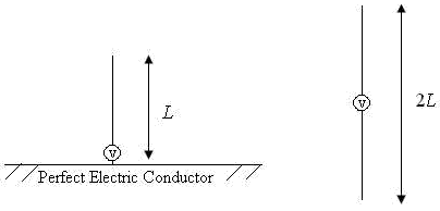 + +The `monopole` antenna consists of a `quarter-wave` length ($$\lambda/4$$) of wire of +length $$L$$ which is connected to the 'hot' `RF` input terminal and a infinitely +large `RF` ground plane conductor which is connected to electrical ground. The +'hot' and `RF` ground elements are electrically separated from each other. + +Most practical `HF` and `VHF` `monopole` antennas are shorter than a quarter +wavelength due to size constraints and are therefore modelled as electrically +small `monopoles` ($$L \leq (1/8)\lambda$$) from this point forward. + +An electrically small `monopole` antenna can be modelled as a series circuit with +the elements shown in the image below. + +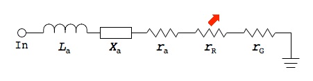 + +$$L_{a}$$ represents the antenna conductor inductance. This is the parasitic +inductance of the active element of the antenna which is just a wire made out of +a material such as copper with a length and diameter. This value is usually very +small and can be neglected. + +The reactance of an electrically short `monopole` ($$L \leq (1/8)\lambda$$) is +represented by $$X_{a}$$ and can be calculated as follows: + +$$ X_{a} = 60(1 - \ln{(\frac{L}{a})})\cot{(2\pi\frac{L}{\lambda})}j \Omega $$ + +This equation originally appears in the "Antenna Engineering Handbook", Third +Edition by `Richard C. Johnson`. + +From the equation above it can be seen that the reactance of an electrically +short `monopole` is primarily capacitive. + +The radius of the wire (active element) in meters is given by $$a$$ and the +operational wavelength is given by $$\lambda$$. The operational wavelength can be +calculated by the transmit frequency ($$f_{t}$$) and the speed of light in a +vacuum ($$c$$): + +$$ \lambda = \frac{c}{f_{t}} $$ + +The loss resistance $$r_{a}$$ is the effective ac resistance of the antenna active +element due to the skin effect. The skin effect is a phenomenon whereby `RF` +current tends to flow near the surface of the conductor as the frequency, and as +a consequence, magnetic field strength at the center of the conductor increases. + +The skin depth is given by: + +$$ \delta = \frac{1}{\sqrt{\pi f_{t} \mu_{0} \sigma}} $$ + +$$\sigma$$ is the conductivity of the active element's composite material (copper) +while $$\mu_{0}$$ is the permeability constant. Once $$\sigma$$ is computed the real +ac resistance can be found as follows: + +$$ r_{a} = \frac{L}{2\pi a \delta \sigma} $$ + +At `VHF` the loss resistance $$r_{a}$$ is also very small and can typically be +neglected. + +The radiation resistance $$r_{R}$$ of an electrically small monopole ($$L \leq +(1/8)\lambda$$) is the effective real resistance that represents the power that +is radiated away from the antenna as electromagnetic waves. For an electrically +short `monopole`, radiation resistance is given by the equation below: + +$$ r_{R} = 40 \pi^2(\frac{L}{\lambda})^2 \Omega $$ + +$$r_{G}$$ represents the losses in the `RF` ground plane and this parameter is +usually neglected. A stable `RF` ground plane is essential for an antenna to +function correctly. An antenna ground plane serves as an `RF` return path for `AC` +displacement current. + +For a `monopole` the ground plane also serves the function of mirroring the active +radiation element to form the second half of the antenna. This derivation is +obtained using image theory and is beyond the scope of this journal entry. + +# S-Parameters + +Most passive `RF` circuits such as filters, matching networks, etc are linear. +That is their output voltage, current and power relationships are derived from a +system of linear equations. Some active devices such as `class-A` `small-signal` +amplifiers are also linear. + +Scattering parameters or `S-parameters` can be used to model the behaviour of +these `linear` `RF` networks when stimulated by a steady-state signal. + +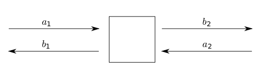 + +The image above depicts a `DUT` 'black box' which we use to derive the scattering +parameters. The network has `2` distinct ports (`port 1`, `port 2`) and 4 scattering +parameters: $$S_{11}, S_{12}$$ and $$S_{21}, S_{22}$$. The scattering parameters are +complex values with both a real and imaginary part. + +We define each scattering parameter in terms of two voltage waves at the input +(`port 1`) and output (`port 2`). Let $$a_{1}, b_{1}$$ represents the incident and +reflected voltage waves at `port 1` while $$a_{2}, b_{2}$$ represent the incident +and reflected voltage waves at `port 2`. + +The S-parameters can then be defined as follows: + +$$ S_{11} = \frac{b_{1}}{a_{1}} = \frac{V_{1}^-}{V_{1}^+}, S_{12} = +\frac{b_{1}}{a_{2}} = \frac{V_{1}^-}{V_{2}^+} $$ + +$$ S_{21} = \frac{b_{2}}{a_{1}} = \frac{V_{2}^-}{V_{1}^+}, S_{22} = +\frac{b_{2}}{a_{2}} = \frac{V_{2}^-}{V_{2}^+} $$ + +It should be mentioned at this point that s-parameters can also be defined in +terms of 'power waves' by considering the complex input impedance of the `DUT`. +However the voltage wave definition is the most popular. + +A system of linear equations can then be derived for $$b_{1}$$ and $$b_{2}$$: + +$$ b_{1} = S_{11}a_{1} + S_{12}a_{2} $$ + +$$ b_{2} = S_{21}a_{1} + S_{22}a_{2} $$ + +Which can be expressed in terms of the `S-parameter` matrix: + +$$ \begin{bmatrix} b_{1} \\ +b_{2} \end{bmatrix} \begin{bmatrix} S_{11} S_{12} \\ +S_{21} S_{22} \end{bmatrix} = \begin{pmatrix} a_{1} \\ +a_{2} \end{pmatrix} $$ + +There are various useful definitions that can be derived from the scattering +parameters. $$S_{21}$$ and $$S_{11}$$ are the most commonly used scattering +paramters. + +The first useful definition is the logarithmic power gain of the network in `dB` +($$G_{p}$$) which can be expressed in terms of $$|S_{21}|$$: + +$$ G_{p} = 20\log_{10}|S_{21}| $$ + +$$S_{11}$$ is related to the input reflection coefficient $$\Gamma_{in}$$ and can be +used to obtain the input impedance of the network $$Z_{in}$$: + +$$ S_{11} = \Gamma_{in} $$ + +$$ Z_{in} = Z_{0} \frac{1+S_{11}}{1-S_{11}} $$ + +The ratio of reflected ($$P_{ref}$$) and incident power ($$P_{inc}$$) at `port 1` is +given by: + +$$ \frac{P_{ref}}{P_{inc}} = |\Gamma_{in}|^2 $$ + +Another useful definition is the input (`port 1`) return loss $$RL_{in}$$: + +$$ RL_{in} = -20\log_{10}(|S_{11}|) $$ + +From the above formula it can be seen that return loss is typically a positive +number (since $$|S11| < 0$$), however sometimes it is quoted as a negative number +in which case the data is referring to the `log` magnitude of $$S_{11}$$ directly +($$-RL_{in}$$), not the actual return loss which is positive as mentioned. + +Return loss for ($$S_{11}$$) is a measure of how well matched `port 1` of the +network is to the reference impedance. A return loss greater than `10dB` is +usually desirable for a good match. + +Another measure of how well matched a network is to the reference impedance is +called `VSWR` (voltage standing wave ratio). The `VSWR` of `port 1` ($$s_{in}$$) is +defined by: + +$$ s_{in} = \frac{1+|S_{11}|}{1-|S_{11}|} $$ + +`VSWR` is typically used to measure the matching conditions of antennas. A +($$s_{in} < 2$$) is generally considered suitable for most antenna applications. + +A `VNA` (Vector Network Analyzer) is an instrument that is used to measure +`S-parameters`. Most affordable commercial `VNA's` are `2-port` `1-path` devices, i.e +they only measure $$S_{11}$$ and $$S_{21}$$ and the `DUT` must therefore be reversed +to obtain $$S_{22}$$ and $$S_{12}$$. + +The input and output impedance obtained for $$S_{11}$$ and $$S_{22}$$ can also be +represented in graphical form as a smith chart. A `smith chart` is a real and +imaginary chart where the imaginary (`y-axis`) axis has been bent around the +`x-axis`. It can be used to plot any value of complex impedance. An example of the +`smith chart` is shown in the figure below. + +The top half of the smith chart represent inductive reactance while the bottom +half represents capacitive reactance. The circles passing through the `x-axis` are +known as constant resistance circles where the left most point on the real axis +of the smith chart represents a short circuit (`SC`) while the rightmost point +represents an open circuit (`OC`). + +For an ideal `50` $$\Omega$$ match there should be a single point in the middle of +the smith chart. + +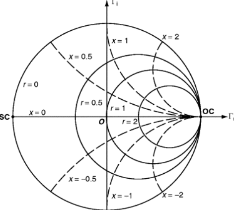{:height="300px"} + +# Harmonic Balance + +`RF` power amplifier's are `large-signal` non-linear devices. + +At this point a distinction is required between small signal and large signal +amplifiers. For `small-signal` amplifiers the input and output power is typically +small and these devices typically operate in their `linear` region. + +`Large-signal`, `class AB`, `B` and `C` devices typically operate with large input and +output power and their response is strongly `non-linear` due to the class of +operation. Therefore for power amplifier classes other than `class A`, +`S-parameters` cannot be used reliably in the design of `RF` power amplifiers. + +Rather a designer relies on vendor supplied `non-linear` software models of the +power amplifier transistor and typically uses a `non-linear` frequency domain +analysis technique such as the harmonic balance method (`HBM`) to characterise the +power amplifier's performance. + +`Harmonic balance` is a frequency domain technique used to calculate the steady +state response of a non-linear circuit. `HBM` can be defined in multiple ways, +however in this case let us demonstrate `HBM` through an example circuit. + +Given a circuit with $$N$$ nodes, let vector $$v$$ represent the respective node +voltages. For ease of representation we model a circuit with capacitors and +voltage controlled resistors. Then applying `KCL` (Kirchoff's Current Law) to the +circuit yields the following systems of equations: + +$$ f(v,t) = i(v(t)) + \frac{d}{dt}q(v(t)) + \int_{-\infty}^t{y(t-\tau)v(\tau)} + +i_{s}(t) = 0 $$ + +We let $$q$$ and $$i$$ represent the sum of the charges and currents entering the +nodes due to the non-linearities. $$y$$ is the impulse response matrix of the +circuit with all non-linearities removed while $$i_{s}$$ represents the external +source currents. + +We then convert equation above into the frequency domain: + +$$ F(V) = I(V) + ZQ(V) + YV + I_{s} = 0 $$ + +Here $$Z$$ represents a matrix with frequency coefficients representing the +differentiation step. The convolution integral in the equation above maps to `YV` +as shown where `Y` is the admittance matrix for the `linear` portion of the circuit. + +`V` then contains the fourier coefficients of the voltage at each $$N$$ nodes at +every harmonic. This process is merely nothing more than `KCL` in the frequency +domain for `non-linear` circuits. + +# Lumped and Distributed Element Networks + +As mentioned above, as the size of a circuit element starts to approach a +fraction (typically `1/10`) of the wavelength of the highest `RF` signal frequency, +the lumped element approximation for the circuit element no longer holds. In +these cases lumped or discrete components cannot be used and so a distributed +element/model must be utilized. + +Traditionally the use of lumped element components at `RF` frequencies is most +common below around `500 MHz`. Above `500 MHz` these lumped circuit +elements become more difficult to design with. + +# Classes Of Operation + +Depending on the `DC` operating point of the power transistor, different values of +efficiency and output power can be obtained for the same input power. Efficiency +is generally considered the most important design parameter for an `RF` power +amplifier. + +In the `class-A` configuration the transistor is biased such that the quiescent +drain current is equal to the peak amplitude of the current expected through the +load. This allows for a symmetrical voltage and current swing at the output and +the transistor conducts for the full `360` degrees of the input waveform. + +The advantages of this configuration are excellent linearity and gain at the +expense of reduced efficiency. A `class-A` power amplifier with an inductively +loaded drain has a maximum theoretical efficiency of `50%`. + +`Class-B` power amplifiers aim to achieve greater efficiency by only conducting +for half of the input drive cycle (`180` degrees). `Class-B` power amplifiers have a +maximum theoretical efficiency of `75%` and the transsitor is biased at cutoff. +Again `class-B` `PA's` can be placed in a single-ended configuration or push-pull. +The advantage of `class-B` are increased efficiency at the expense of decreased +linearity. + +A compromise is thus needed between `class A` and `class B` such that we have +sufficient linearity at a reasonable efficiency. A `class-AB` power amplifier is a +solution to this problem. + +In the `class-AB` mode of operation the transistor is biased with a quiescent +drain current slightly to moderately above cutoff, depending on the linearity +requirements. This improves the linearity of the power amplifier while typically +maintaining an efficiency of `50%` to `70%` in practice. `Class-AB` power +amplifier's have a conduction angle between `180` and `360` degrees. + +The `single-ended`, `class-AB` mode of operation is therefore a popular choice +amongst designers. + +# Stability Analysis + +`RF` power +amplifier's are inherently unstable devices which often require some form of +stabilization to operate correctly. + +Amplifier instability is usually caused by some type of gain and feedback +mechanism. In `MOSFET` transistor's the feedback mechanism is typically due to the +gate to drain capacitance that couples a portion of the output back into the +input and vice versa. This effect often manifests as unwanted oscillation at +either the input and output of the PA. + +Small signal parameters (such as `S-parameters`) are typically used to +characterize stability of `RF` power amplifier's even though these are `non-linear` +devices. This is because small signal models can still provide useful insights +into the design of a `PA` without requiring complex non-linear calculations. +Typically the operation of a `PA` is linearized around an operating point. + +There are various stability factors available to a designer and an amplifier may +be conditionally stable or unconditionally stable. If an amplifier is +conditionally stable then there exists a load and source impedance that causes +the amplifier to oscillate. Therefore unconditional stability is usually +desired. + +The most common stability factor in use is the `Rollet` stability factor ($$K$$) +which is defined as follows: + +$$ K = \frac{1 - |S_{11}|^2 - |S_{22}|^2 + | \Delta |^2}{2|S_{12}S_{21}|} $$ + +Here $$\|\Delta\|$$ is defined as the scattering-matrix determinant: + +$$ | \Delta | = |S_{11}S_{22} - S_{21}S_{12}| $$ + +We define three more stability Criterion in terms of $$\Delta, B_{1}$$ and +$$B_{2}$$: + +$$ B_{1} = 1 + |S_{11}|^2 - |S_{22}|^2 - |\Delta|^2 $$ + +$$ B_{2} = 1 + |S_{22}|^2 - |S_{11}|^2 - |\Delta|^2 $$ + +In order for an amplifier to be conditionally stable we require the +following conditions: + +$$ K \ge 1 $$ + +$$ \Delta < 1 $$ + +$$ B_{1} > 0, B_{2} > 0 $$ + +# Efficiency +The most common measure of `RF` power amplifier efficiency is $$PAE$$ +(power added efficiency) and is defined as follows: + +$$ PAE = \frac{P_{out} - P_{in}}{P_{DC}} $$ + +Here $$P_{in}$$ represents the `RF` input power from the source, $$P_{out}$$ +represents `RF` power delivered to the load and $$P_{DC}$$ represents the total `DC` +power. + +# P1dB Compression Point + +The `P1dB` point is defined as the output power level at which +the gain of an amplifier decreases by `1 dB` from its nominal value which +indicates the onset of gain non-linearity. + +Most amplifier's start to compress approximately `5` to `10 dB` below their `P1dB` +point. + +The `P1dB` point indicates that power amplifier's have a linear and non-linear +region of power gain. + +# Load Pull + +`Load-pull` is an empirical `RF` `PA` design technique in which the +reflection coefficient or impedance presented to the drain of a `RF` power +transistor is varied by an electrical or mechanical impedance tuner to any +arbitrary value. The technique is traditionally used to determine the optimum +load impedance to present to an `RF` power amplifier for maximum output power. + +Once the optimum load impedance is determined the synthesis of matching networks +can then take place. `Load-pull` tuners are expensive devices and are therefore +typically out of the reach of most students or experimenters. + +In the case where a physical `load-pull` tuner is not available and a `non-linear` +model for the chosen `RF` power transistor exists, then a simulated `load-pull` can +be performed. + +# LC Filtering + +As `non-linear` devices, power amplifiers typically produce +harmonic frequency content that must be filtered out in order to comply with +regulatory standards on spurious emissions. `LC` networks can be constructed with +varying number of elements (poles) in order to achieve a specific roll-off in +the stop-band. + +Two types of filter response are commonly used in `RF` circuit design, these are +the `Chebyshev` and `Butterworth` responses. `Chebyshev` `LC` filters typically have a +steeper roll-off but suffer from passband ripple. + +`Butterworth` `LC` filters typically have a flat response in the passband with a +gradual roll-off in the stop band. These types of filters can be designed +manually using filter constants or using `RF` design software such as `Matlab` (`RF +Toolbox`) and typically an optimization algorithm. We typically optomize for +either stopband attenuation or input impedance. + +That concludes this journal entry! I have just touched on some basic principles that +might help with understanding more advanced concepts. + +# Signature + +``` ++---------------------------------------+ +| .-. .-. .-. | +| / \ / \ / \ + | +| \ / \ / \ / | +| "_" "_" "_" | +| | +| _ _ _ _ _ _ ___ ___ _ _ | +| | | | | | | \| | /_\ | _ \ / __| || | | +| | |_| |_| | .` |/ _ \| /_\__ \ __ | | +| |____\___/|_|\_/_/ \_\_|_(_)___/_||_| | +| | +| | +| Lunar RF Labs | +| Email: root@lunar.sh | +| | +| Research Laboratories | +| OpenAlias (BTC, XMR): lunar.sh | +| Copyright (C) 2022-2024 | ++---------------------------------------+ +``` |