1
2
3
4
5
6
7
8
9
10
11
12
13
14
15
16
17
18
19
20
21
22
23
24
25
26
27
28
29
30
31
32
33
34
35
36
37
38
39
40
41
42
43
44
45
46
47
48
49
50
51
52
53
54
55
56
57
58
59
60
61
62
63
64
65
66
67
68
69
70
71
72
73
74
75
76
77
78
79
80
81
82
83
84
85
86
87
88
89
90
91
92
93
94
95
96
97
98
99
100
101
102
103
104
105
106
107
108
109
110
111
112
113
114
115
116
117
118
119
120
121
122
123
124
125
126
127
128
129
130
131
132
133
134
135
136
137
138
139
140
141
142
143
144
145
146
147
148
149
150
151
152
153
154
155
156
157
158
159
160
161
162
163
164
165
166
167
168
169
170
171
172
173
174
175
176
177
178
179
180
181
182
183
184
185
186
187
188
189
190
191
192
193
194
195
196
197
198
199
200
201
202
203
204
205
206
207
208
209
210
211
212
213
214
215
216
217
218
219
220
221
222
223
224
225
226
227
228
229
230
231
232
233
234
235
236
237
238
239
240
241
242
243
244
245
246
247
248
249
250
251
252
253
254
255
256
257
258
259
260
261
262
263
264
265
266
267
268
269
270
271
272
273
274
275
276
277
278
279
280
281
282
283
284
285
286
287
288
289
290
291
292
293
294
295
296
297
298
299
300
301
302
303
304
305
306
307
308
309
310
311
312
313
314
315
316
317
318
319
320
321
322
323
324
325
326
327
328
329
330
331
332
333
334
335
336
337
338
339
340
341
342
343
344
345
346
347
348
349
350
351
352
353
354
355
356
357
358
359
360
361
362
363
364
365
366
367
368
369
370
371
372
373
374
375
376
377
378
379
380
381
382
383
384
385
386
387
388
389
390
391
392
393
394
395
396
397
398
399
400
401
402
403
404
405
406
407
408
409
410
411
412
413
414
415
416
417
418
419
420
421
422
423
424
425
426
427
428
429
430
431
432
433
434
435
436
437
438
439
440
441
442
443
444
445
446
447
448
449
450
451
452
453
454
455
456
457
458
459
460
461
462
463
464
465
466
467
468
469
470
471
472
|
---
layout: post
title: Transistor Circuit Design For Newbies
author: Dylan Müller
---
> `BJTs` are important electronic devices that find use in a wide range of
> applications. Learn how to design circuits with them.
1. [Principle of operation](#principle-of-operation)
3. [Transistor as a switch](#transistor-as-a-switch)
4. [Transistor as an amplifier](#transistor-as-an-amplifier)
5. [LTSpice](#ltspice)
# Principle of Operation
There are various analogies that you will most likely come across when first
learning about transistors, a useful analogy is that of a mechanically
controlled water valve.
{:width="500px"}
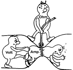
Here it is important to reference the water analogy of current and voltage. In
the water analogy we picture a column of water moving through a pipe.
We define current as the movement of water (`charge`) through the pipe (wire), or
in mathematical terms the rate of flow of water (`charge`) past a given point with
respect to time:
$$ i=\frac{dC}{dt} $$
Voltage is analogous to the pressure differential between two points. For
example, suppose we suspend water in a pipe and then apply a high pressure at
the top and a lower pressure at the bottom. We have just set up a 'water
potential difference' between two points and this tends to move water (`charge`)
from the higher pressure region (voltage) to the lower pressure region.
The higher the water potential, the faster the column of water (`charge`) moves
through the pipe when it has the chance.
In reality, voltage arises due to the presence of electric fields. For a given
electric field between two points, a positive test charge may be placed at any
distance along the electric field lines, that is, its 'field potential' varies
and a positive charge placed closer to the positive end of the electric field
feels more repulsion (and therefore has a higher potential to do work) than at
the negative end of the field.
Potential difference (voltage\) is just a differential measure of this electric
'field potential' or put differently, the capacity of charge to do work in the
presence of an `electric` field:
$$ V_{f} - V_{i} = -\int \overrightarrow{E} \cdot \overrightarrow{d}s $$
With this in mind the idea of a water valve then makes sense. The valve consists
of three ports, one attached to one end of the pipe, the other port to the end
section of the pipe and then the valve itself, sitting in the middle and
regulating the flow of water between both ends.
By rotating the valve we adjust the water flow rate (current) through the pipe.
This is the basic principle of operation of a transistor. However rather than
applying a mechanical torque, we apply a potential difference at the base to
regulate current flow.
You may think of the degree to which the mechanical valve is open or closed as
proportional to the voltage applied at the base of the transistor. This means
that we can control a potentially larger current through the transistor using a
smaller current through the base (through the application of a base voltage),
this is one of the useful properties of transistors.
Bipolar Junction Transistors (`BJTs`) usually consists of three semiconductor
layers which can be of two types: `n` or `p`. The individual `silicon` layers are
crystalline structures that have what are known as dopants added to them. These
are individual elements (`phosphorus`, `boron`) added to neutral `silicon` (and
replace the corresponding `silicon` atoms) in order to change the electrical
properties of the layer.

For example, `boron` `[B]` dopant has a valency (number of outer electrons) of `3`,
while `silicon` has a valency of `4`. This means that when `boron` and `silicon` bond
covalently (sharing of each others electrons) there is a mismatch (`3` < `4`)
between their valence electrons, leaving a 'hole', which needs to be filled with
an electron in order to match `silicon's` valency. This results in a crystal
structure with a net positive charge, the `p` type layer.
In contrast `phosphorus` `[P]` dopant has a valency of `5`, again there is a mismatch
(`5` > `4`) with `silicon's` valency (`4`), allowing for the extra electron of
`phosphorus` to move freely through the crystal structure and giving the overall
crystal layer a negative polarity, the `n` type layer.
{:height="200px"}
If we were to place an `n` region and `p` region together we would form an
electronic device known as a diode. A diode is a `2` terminal device (with the `n`
side connected to the negative terminal (`cathode`) and `p` side connected to the
positive terminal (`anode`) that only allows current flow in one direction.
It is also worth nothing that by placing an `n` and `p` region next to one another
there is a localised effect at their layer boundary that results in a small
number of electrons (from the `n` type region) migrating to the `p` type region in
what is known as the depletion region.
{:height="300px"}
The migration of electrons from the n type region to the `p` type region at the `np`
boundary sets up what is known as a barrier potential, a secondary electric
field at the np layer boundary in opposition to the primary `E-field` (between `p`
and `n`).
This is the amount of voltage (`pressure`) required to force `n` layer electrons
through the `np` barrier (the secondary `E-field`) where they can flow into the
positive terminal (`anode`) of the diode.
It is equivalent to having a water valve initially shut tight and requiring a
torque in order to get water flowing. A typical value for the barrier potential
of garden variety diodes is between `0.3v-0.7v`.

A bipolar junction transistor (`BJT`) may be viewed as a combination of two diodes
(shown below for an `NPN` transistor):

An `NPN` `BJT` transistor has two current paths, one from the collector to emitter
and the other from the base to emitter. The current flow from collector to
emitter represents the water flow in the pipe containing the valve, while the
current flow from base to emitter represents the degree to which the valve is
open or closed.
You might be wondering why conventional (positive) current flows backwards
through the `base-collector` diode (from collector to emitter) for an `NPN`
transistor. As it turns out, current can actually flow in multiple directions
through a diode. However it takes much more voltage to 'push' charge through a
diode in the direction it's meant to block than in the direction it is meant to
flow.
The ratio of `base-emitter` current to `collector-emitter` current is known as ($$\beta$$)
and is an important consideration in the design of circuits using transistors:
$$ I_{c} = \beta I_{B} $$
Both transistor current paths have an associated voltage drop/potential
difference across them.
For the current flow from base to emitter, there is the `base-emitter` voltage
drop $$V_{BE}$$ and from collector to emitter there is the `collector-emitter`
voltage drop $$V_{CE}$$ :
{:height="200px"}
The values of $$V_{CE}$$, $$V_{BE}$$ and $$V_{CB}$$ have predictable
values for the three modes of operation of a transistor, these are:
* **Cut-off** (The transistor acts as an open circuit; valve closed).
$$V_{BE}$$ < `0.7V`
* **Saturation** (The transistor acts as a short circuit; valve completely open).
$$V_{BE}$$ >= `0.7V`
* **Active** (The transistor acts as an amplifier; valve varies between closed
and completely open).
# Transistor as a switch
When using a transistor as a switch we place the transistor into one of two
states: cut-off or saturation.
The following switching circuit is usually employed (with an `NPN` `BJT`) (shown
together with an `LED`):
{:height="300px"}
The circuit is seen consisting of a base current limiting resistor $$R_{B}$$
as well as a `collector-emitter` current limiting resistor $$R_{LIM}$$.
$$R_{B}$$ serves to set up the correct base current, while $$R_{LIM}$$
serves to limit the maximum current through the `LED` (shown in red) when the
transistor is switched fully on (driven into saturation).
To calculate the values for resistors $$R_{B}$$ and $$R_{LIM}$$ we use
the equation relating base current to collector current defined earlier:
$$ I_{c} = \beta I_{B} $$
The first question becomes what collector current $$I_{C}$$ we desire. This
value depends on the device/load you are trying to switch on/off. It is worth
noting that when a transistor is switched fully on (is in saturation mode) the
equivalent circuit (simplified) is as follows (shown without the `LED`, you can
assume the `LED` follows resistor $$R_{C}$$):
{:width="450px"}
Thus at the collector a direct connection to ground is made. However this
connection is not perfect and there is an associated voltage drop from collector
to emitter of typically around `0.2v` ($$V_{CE}$$) rather than `0v`. Determining
the relevant value for $$I_{C}$$ is then just a matter how much current your
load (`LED`in our case) requires.
For example, a typical green led requires around `15mA` of current to light up
brightly so we set $$I_{C}$$ = `15mA`. A green `LED` also typically has a `2v`
drop across it. To calculate $$R_{LIM}$$ we use ohms law:
$$ R_{LIM} = \frac{V_{CC} - V_{LED} - V_{CE}}{I_{DESIRED}} $$
Given the `LED` and collector to emitter voltage drops of `2v` and `0.2v`
respectively, we can further reduce the above expression above to:
$$ R_{LIM} = \frac{V_{CC} - 2 - 0.2}{15 \cdot 10^{-3}} $$
Choosing $$V_{CC}$$ is just a matter of what you have at hand. For example,
a `5v` or `9v` supply would be adequate to drive the transistor into saturation as
long as $$V_{CC} > $$ `0.7v` (due to the base emitter voltage drop) and $$V_{CC} >$$
`2v` (for the led).
Assume $$V_{CC}$$ = `5v`, then $$R_{LIM}$$ = `186.7` $$\Omega$$
In calculating the required base current, we use the transistor's $$\beta$$ value. This
can be found on the transistors datasheet and typically varies from anywhere
between `20` to `200`. The rule of thumb is to use the minimum value of $$\beta$$ for a
specific transistor type. For the standard garden variety `2N2222` transistor, the
minimum value of $$\beta$$ is around `75`. Therefore to calculate $$I_{B}$$, we have:
$$ I_{B} = \frac{I_{C} \cdot SF}{\beta_{min}} = \frac{15mA \cdot 5}{75} = 1mA $$
You might have noticed an additional factor called `SF` for (safety factor). This
is a factor typically around `5-10` that we multiply our calculated $$I_{B}$$
with in order to ensure we drive the transistor into saturation. This gives a
value of around `1mA` for $$I_{B}$$.
Given $$I_{B}$$, calculating $$R_{B}$$ becomes trivial as we know the
voltage across $$R_{B}$$ as: $$V_{CC} - V_{BE}$$ (think of
$$V_{BE}$$ as a `0.7v` diode) and so we apply ohms law once again:
$$ R_{B} = \frac{V_{CC} - V_{BE}}{I_{B}} = \frac{5-0.7}{1 \cdot 10^{-3}} = 4.3k\Omega $$
Now you can connect a switch between the base resistor and Vcc or connect the
base resistor directly to the output of a `5V-TTL` micro-controller in order to
turn the `LED` on and off! The benefit of using a transistor to do that is that we
require a relatively small current (`< 1mA`) in order to switch a much larger
current through the `LED` (`15mA`)!
In conclusion:
1. Determine required collector current $$I_{C}$$.
2. Calculate $$R_{LIM}$$ (ohms law).
3. Calculate $$I_{B}$$ using lowest value for $$\beta$$.
4. Multiply $$I_{B}$$ by safety factor `5-10`.
5. Calculate $$R_{B}$$ (ohms law).
The simple `LED` transistor circuit was modelled in `LTSpice`, with the `LED`
represented as a series voltage source (representing the `2v` voltage drop).:
{:width="400px"}
A simulation of the `DC` operating point of the circuit yielded:
{:height="200px"}
Here we can see the `~1mA` base current ($$I_{b}$$) driving `~15mA` collector
($$I_{C}$$) current. All current values are shown in `S.I` units of amperes
(`A`).
# Transistor as an amplifier
Here we operate the transistor in its active mode to achieve linear
amplification. Linear amplification means that our output should be a
proportional scaling of our input. For example if we feed in a sine wave we
should ideally get a scaled sine wave out, i.e with no distortion/clipping.
There are various circuit configurations used to achieve amplification using
transistors, a useful 'template' is known as common emitter configuration (shown
below with an `NPN` transistor):
{:width="600px"}
Here we model a `20 mVp` (20mV amplitude) sinusoidal signal source with a
resistance of `50` $$\Omega$$, but your input can be practically anything.
It should be noted that there are two electrical 'components' of the above
circuit, these are `AC` (the fluctuating component) and `DC` (the static component).
When analysing a circuit from a `DC` perspective there are a few rules to follow:
* Capacitors become open circuits.
* Inductors become closed circuits.
This means that at the base of `Q1`, `C3` becomes an open connection, i.e the base
of the transistor cannot see signal source `V2` or the `50` $$\Omega$$. resistor.
Additionally, capacitor `C1` becomes an open circuit and therefore has no effect
(it's as if all the capacitors weren't there in the first place).
Capacitor `C3` is known as a `DC` blocking capacitor and is used to remove the `DC`
component of the input signal at the feed point (base of `Q1`). All signals have a
`DC` component:
{:height="300px"}
Effectively `C3` serves to isolate the fluctuating (`AC`) component from the net
signal, that is, we need a signal that moves along the line `y = 0`.
Capacitor `C2` is also a `DC` blocking capacitor and also serves to remove any `DC`
offset at the output of the amplifier.
The role of capacitor `C1` is a bit more involved and requires and understanding
of `AC` circuit analysis, specifically the `AC` signal gain/amplification
$$A_{v}$$ which, for common emitter configuration, is given by:
$$ A_{v} = \frac{z_{out}}{r'e + R_{e}} $$
Here $$z_{out}$$ represents the output impedance of the common-emitter
amplifier which is given by the parallel combination of $$R_{c}$$ and your
load resistance, $$R_{L}$$ (connected to `C2`).
$$ z_{out} = \frac{R_{c} \cdot R_{L}}{R_{c} + R_{L}} $$
From an `AC` perspective:
* Capacitors become short circuits.
* Inductors become open circuits.
* Voltage sources become grounds.
The term $$r'e$$ is known as the transistor's `AC` base-emitter junction resistance
and is given by:
$$ r'e = \frac{25mV}{I_{E}} $$
The introduction of capacitor `C1` nulls out the term $$R_{e}$$ from the
expression for $$A_{v}$$. This is typically done to achieve higher values
of $$A_{v}$$ than would otherwise be possible if resistor $$R_{e}$$ was
still present. For lower, more controlled values of $$A_{v}$$, resistor
$$R_{e}$$ should not be bypassed by capacitor `C1`.
The first step in the design of the amplifier is choosing $$R_{c}$$ such that
$$z_{out}$$ isn't affected by changes in $$R_{L}$$. For example, for a
large value of $$R_{L}$$ choose $$R_{c} \ll R_{L}$$.
For the purposes of our example we assume $$R_{L}$$ = `100` $$k\Omega$$. We then choose
$$R_{c}$$ = `5` $$k\Omega$$
Next we determine the maximum `AC` gain possible given a fixed $$z_{out}$$ :
$$ A_{v} = \frac{0.7(\frac{V_{CC}}{2})}{0.025} $$
It is usually good practice to give `30%` of $$\frac{V_{CC}}{2}$$ to $$R_{e}$$ and `70%` to $$R_{c}$$. Higher
ratios of $$V_{CC}(R_{e})$$ to $$V_{CC}(R_{c})$$ might lead to higher `AC` gain ($$A_{v}$$) but
could sacrifice operational stability as a result.
Given $$V_{CC}$$ = `5V`, we get $$A_{v}$$ = `70`. This is the highest
expected voltage gain for this amplifier.
We know that:
$$ I_{E} \approx I_{C} \approx \frac{0.025 A_{v}}{z_{out}} $$
Thus, given $$A_{v}$$ = `70`, $$z_{out}$$ = `5` $$k\Omega$$ we have $$I_{E}$$ =
`0.35mA`. We are now able to calculate $$R_{e}$$ :
$$ R_{e} = \frac{0.3(\frac{V_{CC}}{2})}{I_{E}} $$
For $$V_{CC}$$ = `5V`, $$I_{E}$$ = `0.35mA` we get $$R_{e} \approx$$ `2.1` $$k\Omega$$.
A useful parameter for common emitter configuration is the `AC` input impedance
(looking in from `C3`) and is given by:
$$ z_{in} = (\frac{1}{R_{1}} + \frac{1}{R_{2}} + \frac{1}{R_{base}})^{-1} $$
Here $$R_{base}$$ represents the AC input impedance of transistor `Q1`
(looking into the base):
$$ R_{base} = \beta \cdot r'e $$
We know how to calculate `r'e` from earlier and we use the minimum value of $$\beta$$ (`75`
for `2N2222`) to calculate $$R_{base}$$ :
$$ R_{base} = 75 \cdot \frac{25}{0.35} $$
Thus $$R_{base}$$ = `5.4` $$k\Omega$$
Returning to our `DC` analysis, we calculate the expected voltage at the
transistor base:
$$ V_{B} = V_{Re} + 0.7 $$
We know that $$V_{Re}$$ is `30%` of $$\frac{V_{CC}}{2}$$, which gives $$V_{B}$$ = `1.45V`.
Now given $$I_{E}$$ = `0.35mA` we can again use our minimum value for $$\beta$$ to
calculate our required base current:
$$ I_{B} = \frac{0.35 mA}{75} $$
Thus $$I_{B}$$ = `4.57uA`
At this point we need to ensure that small changes in the value of base current
(which occur due to variations in $$\beta$$) do not significantly effect the `DC`
operating point of the amplifier circuit.
In order to ensure a stable operating point we 'stiffen' the voltage divider by
ensuring the only a small fraction of the total resistor divider current flows
into the base of transistor `Q1`.
A good rule of thumb is to allow for `1%` of the total divider current to pass
into the base of the transistor.
$$ \frac{1}{100} \cdot I_{R_{1}} = 4.57uA $$
We can therefore assume that $$I_{R1} \approx I_{R2}$$ and solving the
above expression yields $$I_{R2}$$ = `0.456mA`. Since we know the voltage
across $$R_{2}$$ (given by $$V_{B}$$) we can calculate the resistance
value:
$$ R_{2} = \frac{1.45}{0.99(0.456 \cdot 10^{-3})} $$
This gives $$ R_{2} \approx$$ `3.2` $$k\Omega $$. Finally we calculate the value of
$$R_{1}$$ :
$$ R_{1} = \frac{5-1.45}{0.456 \cdot 10^{-3}} $$
$$ R_{1} \approx $$ `7.8` $$ k\Omega $$
The values of capacitors `C3`, `C2` and `C1` are chosen such that the capacitive
reactance (resistance at `AC`) at the desired signal frequency is minimal.
Capacitive reactance is given by:
$$ X_{C} = \frac{1}{2\pi fC} $$
Now that we have all the required component values, we build the circuit in
`LTSpice`:

A simulation of the `DC` operating point was performed:
{:width="500px"}
Here we can see our expected $$V_{base}$$ of around `1.45V` and an emitter
current of around `0.38mA` (instead of `0.35mA`), not too bad! Let's measure the
voltage gain (with the signal source set to a peak amplitude of `1mV` and a `100K`
$$\Omega$$ load attached):
{:width="500px"}
Our output across our load is seen reaching an amplitude of `70mV` and so we have
a voltage gain of `~70`.
# LTSpice
You can download `LTSpice` from
[https://www.analog.com/en/design-center/design-tools-and-calculators/ltspice-simulator.html](https://www.analog.com/en/design-center/design-tools-and-calculators/ltspice-simulator.html)
# Signature
```
+---------------------------------------+
| .-. .-. .-. |
| / \ / \ / \ |
| / \ / \ / \ / |
| \ / \ / \ / |
| "_" "_" "_" |
| |
| _ _ _ _ _ _ ___ ___ _ _ |
| | | | | | | \| | /_\ | _ \ / __| || | |
| | |_| |_| | .` |/ _ \| /_\__ \ __ | |
| |____\___/|_|\_/_/ \_\_|_(_)___/_||_| |
| |
| |
| Lunar RF Labs |
| https://lunar.sh |
| |
| Research Laboratories |
| Copyright (C) 2022-2025 |
| |
+---------------------------------------+
```
|