1
2
3
4
5
6
7
8
9
10
11
12
13
14
15
16
17
18
19
20
21
22
23
24
25
26
27
28
29
30
31
32
33
34
35
36
37
38
39
40
41
42
43
44
45
46
47
48
49
50
51
52
53
54
55
56
57
58
59
60
61
62
63
64
65
66
67
68
69
70
71
72
73
74
75
76
77
78
79
80
81
82
83
84
85
86
87
88
89
90
91
92
93
94
95
96
97
98
99
100
101
102
103
104
105
106
107
108
109
110
111
112
113
114
115
116
117
118
119
120
121
122
123
124
125
126
127
128
129
130
131
132
133
134
135
136
137
138
139
140
141
142
143
144
145
146
147
148
149
150
151
152
153
154
155
156
157
158
159
160
161
162
163
164
165
166
167
168
169
170
171
172
173
174
175
176
177
178
179
180
181
182
183
184
185
186
187
188
189
190
191
192
193
194
195
196
197
198
199
200
201
202
203
204
205
206
207
208
209
210
211
212
213
214
215
216
217
218
219
220
221
222
223
224
225
226
227
228
229
230
231
232
233
234
235
236
237
238
239
240
241
242
243
244
245
246
247
248
249
250
251
252
253
254
255
256
257
258
259
260
261
262
263
264
265
266
267
268
269
270
271
272
273
274
275
276
277
278
279
280
281
282
283
284
285
286
287
288
289
290
291
292
293
294
295
296
297
298
299
300
301
302
303
304
305
306
307
308
309
310
311
312
313
314
315
316
317
318
319
320
321
322
323
324
325
326
327
328
329
330
331
332
333
334
335
336
337
338
339
340
341
342
343
344
345
346
347
348
349
350
351
352
353
354
355
356
357
358
359
360
361
362
363
364
365
366
367
368
369
370
371
372
373
374
375
376
377
378
379
380
381
382
383
384
385
386
387
388
389
390
391
392
393
394
395
396
397
398
399
400
401
402
403
404
405
406
407
408
409
410
411
412
413
414
415
416
417
418
419
420
421
422
423
424
425
426
427
428
429
430
431
432
433
434
435
436
437
438
439
440
441
442
443
444
445
446
447
448
449
450
451
452
453
454
455
456
457
458
459
460
461
462
463
464
465
466
467
468
469
470
471
472
473
474
475
476
477
478
479
480
481
482
483
484
485
486
487
488
489
490
491
492
493
494
495
496
497
498
499
500
501
502
503
504
505
506
507
508
509
510
511
512
513
514
515
516
517
518
519
520
521
522
523
524
525
526
527
528
529
530
531
532
533
534
535
536
537
538
539
540
541
542
543
544
545
546
547
548
549
550
551
552
553
554
555
556
557
558
559
560
561
562
563
564
565
566
567
568
569
570
571
572
573
574
575
576
577
578
579
580
581
582
583
584
585
586
587
588
589
590
591
592
593
594
595
596
597
598
599
600
601
602
603
604
605
606
607
608
609
610
611
612
613
614
615
616
617
618
619
620
621
622
623
624
625
626
627
628
629
630
631
632
633
634
635
636
637
638
639
640
641
642
643
644
645
646
647
648
649
650
651
652
653
654
655
656
657
658
659
660
661
662
663
664
665
666
667
668
669
670
671
672
673
674
675
676
677
678
679
680
681
682
683
684
685
686
687
688
689
690
691
692
693
694
695
696
697
698
699
700
701
702
703
704
705
706
707
708
709
710
711
712
713
714
715
716
717
718
719
720
721
722
723
724
725
726
727
728
729
730
731
732
733
734
735
736
737
738
739
740
741
742
743
744
745
746
747
748
749
750
751
752
753
|
---
layout: post
title: RF Circuit and Power Amplifier Design Basics
author: Dylan Müller
---
> A short primer on some of the basic concepts related to `RF` circuit
> and `RF` power amplifier design.
1. [Average Power](#average-power)
2. [Transmission Lines](#transmission-lines)
3. [Impedance Matching](#impedance-matching)
4. [Electromagnetic Transducers](#electromagnetic-transducers)
5. [S-Parameters](#s-parameters)
6. [Harmonic Balance](#harmonic-balance)
7. [Lumped and Distributed Element Networks](#lumped-and-distributed-element-networks)
8. [Classes Of Operation](#classes-of-operation)
9. [Stability Analysis](#stability-analysis)
10. [Efficiency](#efficiency)
11. [P1dB Compression Point](#p1db-compression-point)
12. [Load Pull](#load-pull)
13. [LC Filtering](#lc-filtering)
# Foreword
The aim of this journal entry is to review some basic technical concepts
pertaining to general `RF` circuit design and modelling as well as `RF` power
amplifier design.
`RF` circuit design is typically not covered in detail at an undergraduate level
and the author hopes that this journal entry will provide some useful
information to readers not familiar with the subject.
# Average Power
In order to be successful in `RF` power amplifier design, it is necessary to
understand `AC` power from both a frequency and time domain perspective.
In the frequency-domain, complex `AC` power ($$S$$) is given by:
$$ S = \overline{V}.\overline{I}^* $$
Where $$\overline{V}$$ and $$\overline{I}$$ are the voltage and current phasors. In
`RF` power amplifier design we are typically concerned with maximizing the real
component of complex power $$\Re(S)$$ which represents power dissipated in a load
such as an antenna (modelled by it's radiation resistance). The imaginary part
of $$S$$ represents reactive power which does not perform any useful work.
Average real power ($$P_{avg}$$) is the industry standard measure of power for `RF`
and `microwave` systems and is measured in the `SI` units of `watts (W)`. Average
power over total time ($$T$$) for a continuous-wave (`CW`) signal is defined by the
following time-domain integral:
$$ P_{avg} = \frac{1}{T} \int\limits_0^T v(t).i(t) dt $$
The terms $$v(t)$$ and $$i(t)$$ can then be expanded:
$$ v(t) = v_{p}sin(2\pi ft), i(t) = i_{p}sin(2\pi ft + \theta) $$
Here $$\theta$$ represents the phase angle between $$i(t)$$ and $$v(t)$$ and ($$v_{p}$$)
and ($$i_{p}$$) represent the peak values of the voltage and current waveforms.
It can be shown that for purely sinusoidal voltage and current waveforms:
$$ P_{avg} = \frac{1}{2}v_{p}i_{p}cos(\theta) $$
Hence maximum real power is obtained when the current and voltage waveforms are
in phase. $$cos (\theta)$$ is commonly referred to as the power factor and this
constant relates real power to apparent power $$\|S\|$$. Apparent power is the
total complex power available to a particular load.
In practice average real power is specified in terms of decibels referenced to `1`
`milliwatt (mW)` ($$dBm$$):
$$ dBm(P) = 10\log_{10}(\frac{P}{1mW}) $$
While relative power is measured in decibels ($$dB$$):
$$ dB(P) = 10\log_{10}(\frac{P}{P_{ref}}) $$
## Transmission Lines
Traditional lumped circuit theory is only applicable to low frequency circuits
as it assumes that wires are lossless with negligible electrical length.
Electrical length is usually measured in terms of multiples of the wavelength
($$\lambda$$) of the highest frequency signal that is conducted over the line.
As a rule of thumb, when the length of a wire is greater or equal to
$$\lambda/10$$, the voltage and current in the wire as a function of position
along the wire will no longer be constant with time and wave-like behaviour such
as reflection and standing waves start becoming important. In these cases
utilizing a distributed model, such as the transmission line, often becomes
necessary.
Let $${u}$$ and $${i}$$ represent the voltage and current along the transmission line as
a function of position and time:
$$ u = u(x,t), i = i(x,t) $$
Then at distance $${x+dx}$$ voltage and current can be expressed with a taylor
series expansion:
$$ u(x + dx) = u(x,t) + \frac{\partial u}{\partial x} dx $$
$$ i(x + dx) = i(x,t) + \frac{\partial i}{\partial x} dx $$
A segment of a traditional transmission line is shown in the figure below. It
consists of a series distributed resistance $$R(x)$$, inductance $$L(x)$$ as well as
segment capacitance $$C(x)$$ and conductance $$G(x)$$. A transmission line is
thought of as a continuous series of these segments.
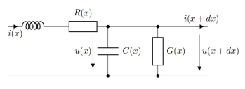
It can be shown that the equations that describe changes in the voltage and
current on the line is given by:
$$ \frac{\partial u}{\partial x} dx = -Ri - L \frac{\partial i}{\partial t} $$
$$ \frac{\partial i}{\partial x} dx = -Gu - C \frac{\partial u}{\partial t} $$
The equations above are known as the telegrapher's equations. These two
equations can be combined to produce two partial differential equations with one
isolated variable each ($${u}$$ or $${i}$$).
$$u$$ and $$i$$ are related by the characteristic impedance ($$Z_{0}$$) of the
transmission line which can be derived from the telegraphers equations:
$$ Z_{0} = \frac{V^+(x)}{I^+(x)} = \sqrt{\frac{R(x)+j\omega L(x)}{G(x)+j\omega
C(x)}} $$
For most transmission lines dielectric and conductor losses are low, so we
assume:
$$ R(x) \ll j\omega L(x), G(x) \ll j\omega C(x) $$
As a result the equation above simplifies to:
$$ Z_{0} = \sqrt{\frac{L(x)}{C(x)}} $$
It is worth noting that characteristic impedance $$Z_{0}$$ of a transmission line
only has an effect at `RF` frequencies. It is not possible to measure the
characteristic impedance of a transmission line directly with a multimeter
because resistance (ohms law) and characteristic impedance (electromagnetic
property) are not the same concept.
Examples of transmission lines include coaxial cable and microstrip line.
Transmission lines typically have a characteristic impedance of `50` $$\Omega$$ in
`RF` systems and are used to carry `RF` signals from one point in a circuit to
another with minimal losses.
# Impedance Matching
It is often said that impedance matching is what truly differentiates `RF` circuit
design from low frequency circuit design. Indeed, it is one of the most common
tasks for an `RF` designer.
`RF` signals travelling along a transmission line can be thought of as
electromagnetic power waves. Power waves are a hypothetical construct, one of
the many possible linear transformations of voltage and current.
The figure below shows a typical `RF circuit` consisting of a `RF` power source
($$G$$) with an impedance of ($$Z_{R}$$) and a load with an impedance of $$Z_{L}$$.
The interface of the generator and load impedance is indicated by the dotted
line.
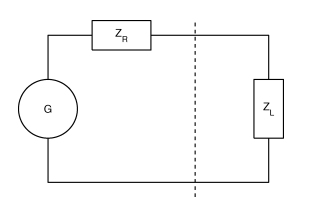
It is at this interface that we experience reflection of the power wave (back to
the generator) when $$Z_{R} \neq Z_{L}$$. If the impedance of the generator and
load were equal then no reflection occurs.
In general, the goal of an `RF` system is to transfer `RF` power as efficiently from
one point to another with minimal reflections. The degree of an electromagnetic
power wave reflected (at the boundary) is determined by the reflection
coefficient ($$\Gamma$$):
$$ \Gamma_{L} = \frac{Z_{L} - Z_{0}}{Z_{L}+Z_{0}} $$
A $$\Gamma$$ of $$0$$ indicates no reflection, while a $$\Gamma$$ of `1` or `-1`
represents total reflection with or without phase inversion.
Here ($$Z_{0}$$) represents the reference impedance of the system which is
typically `50` $$\Omega$$. Maximum power transfer over the boundary from the
generator to the load is only satisfied when:
$$ Z_{L} = Z_{R}^* $$
This expression is known as the conjugate match rule for maximum power transfer.
In most practical `RF` systems $$Z_{L} \neq Z_{R}$$ and so a method of impedance
transformation is required to satisfy the conjugate match rule.
Impedance transformation networks allow a $$Z_{L}$$ with both a real and imaginary
part to be transformed into another complex impedance using reactive components.
Reactive components do not dissipate real power unlike resistors which is why
resistors are rarely used in `RF` impedance matching and filter networks.
The most basic type of impedance transformation network is known as the `LC`
network which consists of an inductor and capacitor. It can be used to transform
a complex load ($$R_{L}$$) to `50` $$\Omega$$. The figure below shows the basic
configuration of the `LC` impedance transformation network.
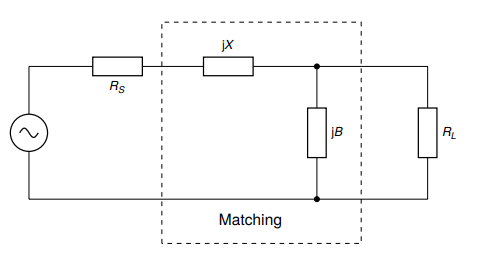
In addition to the `LC` network's impedance transformation property, the `LC`
network can have a low-pass or high-pass response depending on the shunt element
($$jB$$). If it is capacitive then the `LC` network will have a low-pass response or
a high-pass response if it is inductive.
Typically the low pass configuration (with a shunt capacitor) is desired.
It should be noted that the shunt element ($$jB$$) should be placed on the side
with the largest impedance. Therefore there are two possible configurations of
this network:
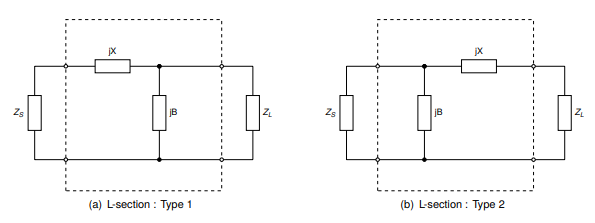
So that type `1` is used when $$R_{L} > R_{S}$$ and type `2` is used when $$R_{L} <
R_{S}$$. Here $$Z_{S}$$ represents $$Z_{0}$$ the system reference impedance $$(50
\Omega)$$.
The design procedure for a type `1` `LC` network is as follows. First we evaluate
the input impedance ($$Z_{in}$$) looking into the matching network.
We start by defining a few variables. Let:
$$ Z_{L} = R_{L} + jX_{L} $$
$$ Z_{S} = Z_{0} = 50 \Omega $$
$$ Z_{in} = jX + \frac{1}{(jB)^{-1} + (Z_{L})^{-1}} $$
Matching conditions are met when $$Z_{in} = Z_{S} = Z_{0}$$.
The equation above can be simplified and separated into real and imaginary
parts:
$$ B(X + X_{L}) = -(Z_{0}R_{L}-XX_{L}) $$
$$ B(R_{L} - Z_{0}) = Z_{0}X_{L} - R_{L}X $$
`B` can then be solved using the following equation:
$$ B = -\frac{R_{L}^2+X_{L}^2}{X_{L} + \sqrt{\frac{R_{L}}{Z_{0}}} \sqrt{R_{L}^2 + X_{L}^2 - Z_{0}R_{L}}} $$
Once `B` is obtained, X may be found by rearranging for `X`:
$$ X = \frac{B(R_{L} - Z_{0}) - Z_{0}X_{L}}{-R_{L}} $$
The figure below depicts the second variant of the `LC` matching network.
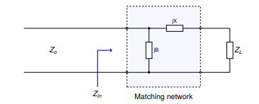
Let:
$$ Z_{L} = R_{L} + jX_{L} $$
$$ Z_{S} = Z_{0} = 50 \Omega $$
$$ Z_{in} = \frac{1}{(jB)^{-1} + (Z_{L} + jX)^{-1}} $$
Matching conditions are met when $$Z_{in} = Z_{S} = Z_{0}$$.
The equation above can be simplified and separated into real and imaginary
parts:
$$ B(X_{L} + X) = -Z_{0}R_{L} $$
$$ B(Z_{0} - R_{L}) = -Z_{0}(X_{L}+X) $$
Again, B can then be solved using the following equation:
$$ B = -Z_{0}\sqrt{\frac{R_{L}}{Z_{0}- R_{L}}} $$
Again, `X` may be found by rearranging for $$(X_{L} + X)$$ and substituting to
yield:
$$ X = \sqrt{R_{L}(Z_{0} - R_{L})} - X_{L} $$
For both `LC` circuit types it is assumed that $$jB$$ represents a capacitive
element and $$jX$$ represents an inductive element so that a low-pass response is
obtained.
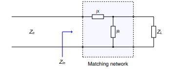
Matching networks with more than two reactive elements also exist. These include
the $$\pi$$-section and `T-section` matching networks that contain `3` reactive
elements each. The figure below depicts the $$\pi$$-section network.
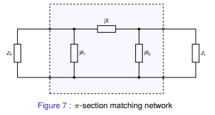
The $$\pi$$-section network is made up of a type `2` `LC` matching network in cascade
with a type 1 `LC` matching network. The central element $$jX$$ is the sum of the
inductive reactance ($$jX$$) of each `LC` matching section, which is combined into a
single reactance.
A virtual load resistance $$R_{x}$$ is interposed in-between the two `LC` matching
networks. The goal of the first `LC` matching network is to then match the source
$$Z_{S}$$ to $$R_{x}$$ while the second `LC` matching network matches $$R_{x}$$ to
$$Z_{L}$$.
The value of $$R_{x}$$ is chosen according to the desired `Q-factor` and must be
smaller than $$R_{L}$$ and $$R_{S}$$. The `Q-factor` of a matching network describes
how well power is transferred from source to load as you deviate from the
designed center frequency of the matching network ($$f_{0}$$).
Is it defined as follows:
$$ Q = \frac{f_{0}}{B} $$
Here $$f_{0}$$ represents the center frequency of the matching network and B
represents the total bandwidth over which no greater than `3dB` of power is lost
from source to load.
A high `Q-factor` is often desirable for a narrowband matching network. It should
be mentioned that the `Q-factor` cannot be controlled with a simple 2 element `LC`
matching network (which id determined by $$R_{L}$$ and $$R_{S}$$). This is one of
the advantages of the $$\pi$$-section matching network.
The `Q-factor` for the $$\pi$$-section filter is given by:
$$ Q_{\pi} = \sqrt{\frac{\max(R_{S}, R_{L})}{R_{x}} - 1} $$
Here `max()` is a function that returns the maximum of two values. Hence the
`Q-factor` of a $$\pi$$-section matching network will be determined by the `LC`
matching section with the highest `Q-factor`.
# Electromagnetic Transducers
Once the necessary `RF` power has been generated and transmitted over various
transmission lines and matching networks it then becomes necessary to convert
this `RF` power into electromagnetic waves which can start propagating through
free space to reach a receiver. For this purpose we use an electromagnetic
transducer known as an antenna.
An antenna can be also be thought of as an impedance transformation network that
matches an `RF` circuit (`50` $$\Omega$$ typical) to free space (`377` $$\Omega$$).
An antenna can be as simple as a piece of wire connected to an `RF` output port
but the efficiency of the antenna in this case would be very low. The two most
common types of antenna's are the `monopole` and `dipole` antenna (shown below).
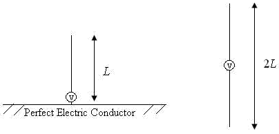
The `monopole` antenna consists of a `quarter-wave` length ($$\lambda/4$$) of wire of
length $$L$$ which is connected to the 'hot' `RF` input terminal and a infinitely
large `RF` ground plane conductor which is connected to electrical ground. The
'hot' and `RF` ground elements are electrically separated from each other.
Most practical `HF` and `VHF` `monopole` antennas are shorter than a quarter
wavelength due to size constraints and are therefore modelled as electrically
small `monopoles` ($$L \leq (1/8)\lambda$$) from this point forward.
An electrically small `monopole` antenna can be modelled as a series circuit with
the elements shown in the image below.
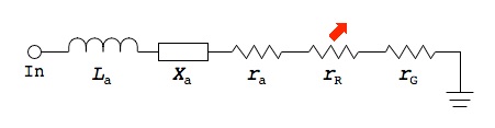
$$L_{a}$$ represents the antenna conductor inductance. This is the parasitic
inductance of the active element of the antenna which is just a wire made out of
a material such as copper with a length and diameter. This value is usually very
small and can be neglected.
The reactance of an electrically short `monopole` ($$L \leq (1/8)\lambda$$) is
represented by $$X_{a}$$ and can be calculated as follows:
$$ X_{a} = 60(1 - \ln{(\frac{L}{a})})\cot{(2\pi\frac{L}{\lambda})}j \Omega $$
This equation originally appears in the "Antenna Engineering Handbook", Third
Edition by `Richard C. Johnson`.
From the equation above it can be seen that the reactance of an electrically
short `monopole` is primarily capacitive.
The radius of the wire (active element) in meters is given by $$a$$ and the
operational wavelength is given by $$\lambda$$. The operational wavelength can be
calculated by the transmit frequency ($$f_{t}$$) and the speed of light in a
vacuum ($$c$$):
$$ \lambda = \frac{c}{f_{t}} $$
The loss resistance $$r_{a}$$ is the effective ac resistance of the antenna active
element due to the skin effect. The skin effect is a phenomenon whereby `RF`
current tends to flow near the surface of the conductor as the frequency, and as
a consequence, magnetic field strength at the center of the conductor increases.
The skin depth is given by:
$$ \delta = \frac{1}{\sqrt{\pi f_{t} \mu_{0} \sigma}} $$
$$\sigma$$ is the conductivity of the active element's composite material (copper)
while $$\mu_{0}$$ is the permeability constant. Once $$\sigma$$ is computed the real
ac resistance can be found as follows:
$$ r_{a} = \frac{L}{2\pi a \delta \sigma} $$
At `VHF` the loss resistance $$r_{a}$$ is also very small and can typically be
neglected.
The radiation resistance $$r_{R}$$ of an electrically small monopole ($$L \leq
(1/8)\lambda$$) is the effective real resistance that represents the power that
is radiated away from the antenna as electromagnetic waves. For an electrically
short `monopole`, radiation resistance is given by the equation below:
$$ r_{R} = 40 \pi^2(\frac{L}{\lambda})^2 \Omega $$
$$r_{G}$$ represents the losses in the `RF` ground plane and this parameter is
usually neglected. A stable `RF` ground plane is essential for an antenna to
function correctly. An antenna ground plane serves as an `RF` return path for `AC`
displacement current.
For a `monopole` the ground plane also serves the function of mirroring the active
radiation element to form the second half of the antenna. This derivation is
obtained using image theory and is beyond the scope of this journal entry.
# S-Parameters
Most passive `RF` circuits such as filters, matching networks, etc are linear.
That is their output voltage, current and power relationships are derived from a
system of linear equations. Some active devices such as `class-A` `small-signal`
amplifiers are also linear.
Scattering parameters or `S-parameters` can be used to model the behaviour of
these `linear` `RF` networks when stimulated by a steady-state signal.
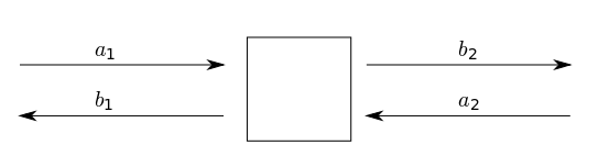
The image above depicts a `DUT` 'black box' which we use to derive the scattering
parameters. The network has `2` distinct ports (`port 1`, `port 2`) and 4 scattering
parameters: $$S_{11}, S_{12}$$ and $$S_{21}, S_{22}$$. The scattering parameters are
complex values with both a real and imaginary part.
We define each scattering parameter in terms of two voltage waves at the input
(`port 1`) and output (`port 2`). Let $$a_{1}, b_{1}$$ represents the incident and
reflected voltage waves at `port 1` while $$a_{2}, b_{2}$$ represent the incident
and reflected voltage waves at `port 2`.
The S-parameters can then be defined as follows:
$$ S_{11} = \frac{b_{1}}{a_{1}} = \frac{V_{1}^-}{V_{1}^+}, S_{12} =
\frac{b_{1}}{a_{2}} = \frac{V_{1}^-}{V_{2}^+} $$
$$ S_{21} = \frac{b_{2}}{a_{1}} = \frac{V_{2}^-}{V_{1}^+}, S_{22} =
\frac{b_{2}}{a_{2}} = \frac{V_{2}^-}{V_{2}^+} $$
It should be mentioned at this point that s-parameters can also be defined in
terms of 'power waves' by considering the complex input impedance of the `DUT`.
However the voltage wave definition is the most popular.
A system of linear equations can then be derived for $$b_{1}$$ and $$b_{2}$$:
$$ b_{1} = S_{11}a_{1} + S_{12}a_{2} $$
$$ b_{2} = S_{21}a_{1} + S_{22}a_{2} $$
Which can be expressed in terms of the `S-parameter` matrix:
$$ \begin{bmatrix} b_{1} \\
b_{2} \end{bmatrix} \begin{bmatrix} S_{11} S_{12} \\
S_{21} S_{22} \end{bmatrix} = \begin{pmatrix} a_{1} \\
a_{2} \end{pmatrix} $$
There are various useful definitions that can be derived from the scattering
parameters. $$S_{21}$$ and $$S_{11}$$ are the most commonly used scattering
paramters.
The first useful definition is the logarithmic power gain of the network in `dB`
($$G_{p}$$) which can be expressed in terms of $$|S_{21}|$$:
$$ G_{p} = 20\log_{10}|S_{21}| $$
$$S_{11}$$ is related to the input reflection coefficient $$\Gamma_{in}$$ and can be
used to obtain the input impedance of the network $$Z_{in}$$:
$$ S_{11} = \Gamma_{in} $$
$$ Z_{in} = Z_{0} \frac{1+S_{11}}{1-S_{11}} $$
The ratio of reflected ($$P_{ref}$$) and incident power ($$P_{inc}$$) at `port 1` is
given by:
$$ \frac{P_{ref}}{P_{inc}} = |\Gamma_{in}|^2 $$
Another useful definition is the input (`port 1`) return loss $$RL_{in}$$:
$$ RL_{in} = -20\log_{10}(|S_{11}|) $$
From the above formula it can be seen that return loss is typically a positive
number (since $$|S11| < 0$$), however sometimes it is quoted as a negative number
in which case the data is referring to the `log` magnitude of $$S_{11}$$ directly
($$-RL_{in}$$), not the actual return loss which is positive as mentioned.
Return loss for ($$S_{11}$$) is a measure of how well matched `port 1` of the
network is to the reference impedance. A return loss greater than `10dB` is
usually desirable for a good match.
Another measure of how well matched a network is to the reference impedance is
called `VSWR` (voltage standing wave ratio). The `VSWR` of `port 1` ($$s_{in}$$) is
defined by:
$$ s_{in} = \frac{1+|S_{11}|}{1-|S_{11}|} $$
`VSWR` is typically used to measure the matching conditions of antennas. A
($$s_{in} < 2$$) is generally considered suitable for most antenna applications.
A `VNA` (Vector Network Analyzer) is an instrument that is used to measure
`S-parameters`. Most affordable commercial `VNA's` are `2-port` `1-path` devices, i.e
they only measure $$S_{11}$$ and $$S_{21}$$ and the `DUT` must therefore be reversed
to obtain $$S_{22}$$ and $$S_{12}$$.
The input and output impedance obtained for $$S_{11}$$ and $$S_{22}$$ can also be
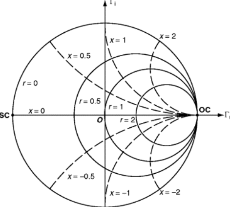
represented in graphical form as a smith chart. A `smith chart` is a real and
imaginary chart where the imaginary (`y-axis`) axis has been bent around the
`x-axis`. It can be used to plot any value of complex impedance. An example of the
`smith chart` is shown in the figure below.
The top half of the smith chart represent inductive reactance while the bottom
half represents capacitive reactance. The circles passing through the `x-axis` are
known as constant resistance circles where the left most point on the real axis
of the smith chart represents a short circuit (`SC`) while the rightmost point
represents an open circuit (`OC`).
For an ideal `50` $$\Omega$$ match there should be a single point in the middle of
the smith chart.
{:height="300px"}
# Harmonic Balance
`RF` power amplifier's are `large-signal` non-linear devices.
At this point a distinction is required between small signal and large signal
amplifiers. For `small-signal` amplifiers the input and output power is typically
small and these devices typically operate in their `linear` region.
`Large-signal`, `class AB`, `B` and `C` devices typically operate with large input and
output power and their response is strongly `non-linear` due to the class of
operation. Therefore for power amplifier classes other than `class A`,
`S-parameters` cannot be used reliably in the design of `RF` power amplifiers.
Rather a designer relies on vendor supplied `non-linear` software models of the
power amplifier transistor and typically uses a `non-linear` frequency domain
analysis technique such as the harmonic balance method (`HBM`) to characterise the
power amplifier's performance.
`Harmonic balance` is a frequency domain technique used to calculate the steady
state response of a non-linear circuit. `HBM` can be defined in multiple ways,
however in this case let us demonstrate `HBM` through an example circuit.
Given a circuit with $$N$$ nodes, let vector $$v$$ represent the respective node
voltages. For ease of representation we model a circuit with capacitors and
voltage controlled resistors. Then applying `KCL` (Kirchoff's Current Law) to the
circuit yields the following systems of equations:
$$ f(v,t) = i(v(t)) + \frac{d}{dt}q(v(t)) + \int_{-\infty}^t{y(t-\tau)v(\tau)} +
i_{s}(t) = 0 $$
We let $$q$$ and $$i$$ represent the sum of the charges and currents entering the
nodes due to the non-linearities. $$y$$ is the impulse response matrix of the
circuit with all non-linearities removed while $$i_{s}$$ represents the external
source currents.
We then convert equation above into the frequency domain:
$$ F(V) = I(V) + ZQ(V) + YV + I_{s} = 0 $$
Here $$Z$$ represents a matrix with frequency coefficients representing the
differentiation step. The convolution integral in the equation above maps to `YV`
as shown where `Y` is the admittance matrix for the `linear` portion of the circuit.
`V` then contains the fourier coefficients of the voltage at each $$N$$ nodes at
every harmonic. This process is merely nothing more than `KCL` in the frequency
domain for `non-linear` circuits.
# Lumped and Distributed Element Networks
As mentioned above, as the size of a circuit element starts to approach a
fraction (typically `1/10`) of the wavelength of the highest `RF` signal frequency,
the lumped element approximation for the circuit element no longer holds. In
these cases lumped or discrete components cannot be used and so a distributed
element/model must be utilized.
Traditionally the use of lumped element components at `RF` frequencies is most
common below around `500 MHz`. Above `500 MHz` these lumped circuit
elements become more difficult to design with.
# Classes Of Operation
Depending on the `DC` operating point of the power transistor, different values of
efficiency and output power can be obtained for the same input power. Efficiency
is generally considered the most important design parameter for an `RF` power
amplifier.
In the `class-A` configuration the transistor is biased such that the quiescent
drain current is equal to the peak amplitude of the current expected through the
load. This allows for a symmetrical voltage and current swing at the output and
the transistor conducts for the full `360` degrees of the input waveform.
The advantages of this configuration are excellent linearity and gain at the
expense of reduced efficiency. A `class-A` power amplifier with an inductively
loaded drain has a maximum theoretical efficiency of `50%`.
`Class-B` power amplifiers aim to achieve greater efficiency by only conducting
for half of the input drive cycle (`180` degrees). `Class-B` power amplifiers have a
maximum theoretical efficiency of `75%` and the transsitor is biased at cutoff.
Again `class-B` `PA's` can be placed in a single-ended configuration or push-pull.
The advantage of `class-B` are increased efficiency at the expense of decreased
linearity.
A compromise is thus needed between `class A` and `class B` such that we have
sufficient linearity at a reasonable efficiency. A `class-AB` power amplifier is a
solution to this problem.
In the `class-AB` mode of operation the transistor is biased with a quiescent
drain current slightly to moderately above cutoff, depending on the linearity
requirements. This improves the linearity of the power amplifier while typically
maintaining an efficiency of `50%` to `70%` in practice. `Class-AB` power
amplifier's have a conduction angle between `180` and `360` degrees.
The `single-ended`, `class-AB` mode of operation is therefore a popular choice
amongst designers.
# Stability Analysis
`RF` power
amplifier's are inherently unstable devices which often require some form of
stabilization to operate correctly.
Amplifier instability is usually caused by some type of gain and feedback
mechanism. In `MOSFET` transistor's the feedback mechanism is typically due to the
gate to drain capacitance that couples a portion of the output back into the
input and vice versa. This effect often manifests as unwanted oscillation at
either the input and output of the PA.
Small signal parameters (such as `S-parameters`) are typically used to
characterize stability of `RF` power amplifier's even though these are `non-linear`
devices. This is because small signal models can still provide useful insights
into the design of a `PA` without requiring complex non-linear calculations.
Typically the operation of a `PA` is linearized around an operating point.
There are various stability factors available to a designer and an amplifier may
be conditionally stable or unconditionally stable. If an amplifier is
conditionally stable then there exists a load and source impedance that causes
the amplifier to oscillate. Therefore unconditional stability is usually
desired.
The most common stability factor in use is the `Rollet` stability factor ($$K$$)
which is defined as follows:
$$ K = \frac{1 - |S_{11}|^2 - |S_{22}|^2 + | \Delta |^2}{2|S_{12}S_{21}|} $$
Here $$\|\Delta\|$$ is defined as the scattering-matrix determinant:
$$ | \Delta | = |S_{11}S_{22} - S_{21}S_{12}| $$
We define three more stability Criterion in terms of $$\Delta, B_{1}$$ and
$$B_{2}$$:
$$ B_{1} = 1 + |S_{11}|^2 - |S_{22}|^2 - |\Delta|^2 $$
$$ B_{2} = 1 + |S_{22}|^2 - |S_{11}|^2 - |\Delta|^2 $$
In order for an amplifier to be conditionally stable we require the
following conditions:
$$ K \ge 1 $$
$$ \Delta < 1 $$
$$ B_{1} > 0, B_{2} > 0 $$
# Efficiency
The most common measure of `RF` power amplifier efficiency is $$PAE$$
(power added efficiency) and is defined as follows:
$$ PAE = \frac{P_{out} - P_{in}}{P_{DC}} $$
Here $$P_{in}$$ represents the `RF` input power from the source, $$P_{out}$$
represents `RF` power delivered to the load and $$P_{DC}$$ represents the total `DC`
power.
# P1dB Compression Point
The `P1dB` point is defined as the output power level at which
the gain of an amplifier decreases by `1 dB` from its nominal value which
indicates the onset of gain non-linearity.
Most amplifier's start to compress approximately `5` to `10 dB` below their `P1dB`
point.
The `P1dB` point indicates that power amplifier's have a linear and non-linear
region of power gain.
# Load Pull
`Load-pull` is an empirical `RF` `PA` design technique in which the
reflection coefficient or impedance presented to the drain of a `RF` power
transistor is varied by an electrical or mechanical impedance tuner to any
arbitrary value. The technique is traditionally used to determine the optimum
load impedance to present to an `RF` power amplifier for maximum output power.
Once the optimum load impedance is determined the synthesis of matching networks
can then take place. `Load-pull` tuners are expensive devices and are therefore
typically out of the reach of most students or experimenters.
In the case where a physical `load-pull` tuner is not available and a `non-linear`
model for the chosen `RF` power transistor exists, then a simulated `load-pull` can
be performed.
# LC Filtering
As `non-linear` devices, power amplifiers typically produce
harmonic frequency content that must be filtered out in order to comply with
regulatory standards on spurious emissions. `LC` networks can be constructed with
varying number of elements (poles) in order to achieve a specific roll-off in
the stop-band.
Two types of filter response are commonly used in `RF` circuit design, these are
the `Chebyshev` and `Butterworth` responses. `Chebyshev` `LC` filters typically have a
steeper roll-off but suffer from passband ripple.
`Butterworth` `LC` filters typically have a flat response in the passband with a
gradual roll-off in the stop band. These types of filters can be designed
manually using filter constants or using `RF` design software such as `Matlab` (`RF
Toolbox`) and typically an optimization algorithm. We typically optomize for
either stopband attenuation or input impedance.
That concludes this journal entry! I have just touched on some basic principles that
might help with understanding more advanced concepts.
# Signature
```
+---------------------------------------+
| .-. .-. .-. |
| / \ / \ / \ |
| / \ / \ / \ / |
| \ / \ / \ / |
| "_" "_" "_" |
| |
| _ _ _ _ _ _ ___ ___ _ _ |
| | | | | | | \| | /_\ | _ \ / __| || | |
| | |_| |_| | .` |/ _ \| /_\__ \ __ | |
| |____\___/|_|\_/_/ \_\_|_(_)___/_||_| |
| |
| |
| Lunar RF Labs |
| https://lunar.sh |
| |
| Research Laboratories |
| Copyright (C) 2022-2025 |
| |
+---------------------------------------+
```
|