diff options
Diffstat (limited to '_posts/2020-11-03-transistor-design-for-newbies.md')
| -rw-r--r-- | _posts/2020-11-03-transistor-design-for-newbies.md | 472 |
1 files changed, 472 insertions, 0 deletions
diff --git a/_posts/2020-11-03-transistor-design-for-newbies.md b/_posts/2020-11-03-transistor-design-for-newbies.md new file mode 100644 index 0000000..d473fed --- /dev/null +++ b/_posts/2020-11-03-transistor-design-for-newbies.md @@ -0,0 +1,472 @@ +--- +layout: post +title: Transistor Circuit Design For Newbies +author: Dylan Müller +--- + +> `BJTs` are important electronic devices that find use in a wide range of +> applications. Learn how to design circuits with them. + +1. [Principle of operation](#principle-of-operation) +3. [Transistor as a switch](#transistor-as-a-switch) +4. [Transistor as an amplifier](#transistor-as-an-amplifier) +5. [LTSpice](#ltspice) + +# Principle of Operation + +There are various analogies that you will most likely come across when first +learning about transistors, a useful analogy is that of a mechanically +controlled water valve. + +{:width="500px"} + +Here it is important to reference the water analogy of current and voltage. In +the water analogy we picture a column of water moving through a pipe. + +We define current as the movement of water (`charge`) through the pipe (wire), or +in mathematical terms the rate of flow of water (`charge`) past a given point with +respect to time: + +$$ i=\frac{dC}{dt} $$ + +Voltage is analogous to the pressure differential between two points. For +example, suppose we suspend water in a pipe and then apply a high pressure at +the top and a lower pressure at the bottom. We have just set up a 'water +potential difference' between two points and this tends to move water (`charge`) +from the higher pressure region (voltage) to the lower pressure region. + +The higher the water potential, the faster the column of water (`charge`) moves +through the pipe when it has the chance. + +In reality, voltage arises due to the presence of electric fields. For a given +electric field between two points, a positive test charge may be placed at any +distance along the electric field lines, that is, its 'field potential' varies +and a positive charge placed closer to the positive end of the electric field +feels more repulsion (and therefore has a higher potential to do work) than at +the negative end of the field. + +Potential difference (voltage\) is just a differential measure of this electric +'field potential' or put differently, the capacity of charge to do work in the +presence of an `electric` field: + +$$ V_{f} - V_{i} = -\int \overrightarrow{E} \cdot \overrightarrow{d}s $$ + +With this in mind the idea of a water valve then makes sense. The valve consists +of three ports, one attached to one end of the pipe, the other port to the end +section of the pipe and then the valve itself, sitting in the middle and +regulating the flow of water between both ends. + +By rotating the valve we adjust the water flow rate (current) through the pipe. +This is the basic principle of operation of a transistor. However rather than +applying a mechanical torque, we apply a potential difference at the base to +regulate current flow. + +You may think of the degree to which the mechanical valve is open or closed as +proportional to the voltage applied at the base of the transistor. This means +that we can control a potentially larger current through the transistor using a +smaller current through the base (through the application of a base voltage), +this is one of the useful properties of transistors. + +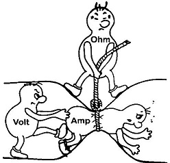 + +Bipolar Junction Transistors (`BJTs`) usually consists of three semiconductor +layers which can be of two types: `n` or `p`. The individual `silicon` layers are +crystalline structures that have what are known as dopants added to them. These +are individual elements (`phosphorus`, `boron`) added to neutral `silicon` (and +replace the corresponding `silicon` atoms) in order to change the electrical +properties of the layer. + + + +For example, `boron` `[B]` dopant has a valency (number of outer electrons) of `3`, +while `silicon` has a valency of `4`. This means that when `boron` and `silicon` bond +covalently (sharing of each others electrons) there is a mismatch (`3` < `4`) +between their valence electrons, leaving a 'hole', which needs to be filled with +an electron in order to match `silicon's` valency. This results in a crystal +structure with a net positive charge, the `p` type layer. + +In contrast `phosphorus` `[P]` dopant has a valency of `5`, again there is a mismatch +(`5` > `4`) with `silicon's` valency (`4`), allowing for the extra electron of +`phosphorus` to move freely through the crystal structure and giving the overall +crystal layer a negative polarity, the `n` type layer. + +{:height="200px"} + +If we were to place an `n` region and `p` region together we would form an +electronic device known as a diode. A diode is a `2` terminal device (with the `n` +side connected to the negative terminal (`cathode`) and `p` side connected to the +positive terminal (`anode`) that only allows current flow in one direction. + +It is also worth nothing that by placing an `n` and `p` region next to one another +there is a localised effect at their layer boundary that results in a small +number of electrons (from the `n` type region) migrating to the `p` type region in +what is known as the depletion region. + +{:height="300px"} + +The migration of electrons from the n type region to the `p` type region at the `np` +boundary sets up what is known as a barrier potential, a secondary electric +field at the np layer boundary in opposition to the primary `E-field` (between `p` +and `n`). + +This is the amount of voltage (`pressure`) required to force `n` layer electrons +through the `np` barrier (the secondary `E-field`) where they can flow into the +positive terminal (`anode`) of the diode. + +It is equivalent to having a water valve initially shut tight and requiring a +torque in order to get water flowing. A typical value for the barrier potential +of garden variety diodes is between `0.3v-0.7v`. + + + +A bipolar junction transistor (`BJT`) may be viewed as a combination of two diodes +(shown below for an `NPN` transistor): + + + +An `NPN` `BJT` transistor has two current paths, one from the collector to emitter +and the other from the base to emitter. The current flow from collector to +emitter represents the water flow in the pipe containing the valve, while the +current flow from base to emitter represents the degree to which the valve is +open or closed. + +You might be wondering why conventional (positive) current flows backwards +through the `base-collector` diode (from collector to emitter) for an `NPN` +transistor. As it turns out, current can actually flow in multiple directions +through a diode. However it takes much more voltage to 'push' charge through a +diode in the direction it's meant to block than in the direction it is meant to +flow. + +The ratio of `base-emitter` current to `collector-emitter` current is known as ($$\beta$$) +and is an important consideration in the design of circuits using transistors: + +$$ I_{c} = \beta I_{B} $$ + +Both transistor current paths have an associated voltage drop/potential +difference across them. + +For the current flow from base to emitter, there is the `base-emitter` voltage +drop $$V_{BE}$$ and from collector to emitter there is the `collector-emitter` +voltage drop $$V_{CE}$$ : + +{:height="200px"} + +The values of $$V_{CE}$$, $$V_{BE}$$ and $$V_{CB}$$ have predictable +values for the three modes of operation of a transistor, these are: + +* **Cut-off** (The transistor acts as an open circuit; valve closed). + $$V_{BE}$$ < `0.7V` +* **Saturation** (The transistor acts as a short circuit; valve completely open). + $$V_{BE}$$ >= `0.7V` +* **Active** (The transistor acts as an amplifier; valve varies between closed + and completely open). + +# Transistor as a switch + +When using a transistor as a switch we place the transistor into one of two +states: cut-off or saturation. + +The following switching circuit is usually employed (with an `NPN` `BJT`) (shown +together with an `LED`): + +{:height="300px"} + + +The circuit is seen consisting of a base current limiting resistor $$R_{B}$$ +as well as a `collector-emitter` current limiting resistor $$R_{LIM}$$. + +$$R_{B}$$ serves to set up the correct base current, while $$R_{LIM}$$ +serves to limit the maximum current through the `LED` (shown in red) when the +transistor is switched fully on (driven into saturation). + +To calculate the values for resistors $$R_{B}$$ and $$R_{LIM}$$ we use +the equation relating base current to collector current defined earlier: + +$$ I_{c} = \beta I_{B} $$ + +The first question becomes what collector current $$I_{C}$$ we desire. This +value depends on the device/load you are trying to switch on/off. It is worth +noting that when a transistor is switched fully on (is in saturation mode) the +equivalent circuit (simplified) is as follows (shown without the `LED`, you can +assume the `LED` follows resistor $$R_{C}$$): + +{:width="450px"} + +Thus at the collector a direct connection to ground is made. However this +connection is not perfect and there is an associated voltage drop from collector +to emitter of typically around `0.2v` ($$V_{CE}$$) rather than `0v`. Determining +the relevant value for $$I_{C}$$ is then just a matter how much current your +load (`LED`in our case) requires. + +For example, a typical green led requires around `15mA` of current to light up +brightly so we set $$I_{C}$$ = `15mA`. A green `LED` also typically has a `2v` +drop across it. To calculate $$R_{LIM}$$ we use ohms law: + +$$ R_{LIM} = \frac{V_{CC} - V_{LED} - V_{CE}}{I_{DESIRED}} $$ + +Given the `LED` and collector to emitter voltage drops of `2v` and `0.2v` +respectively, we can further reduce the above expression above to: + +$$ R_{LIM} = \frac{V_{CC} - 2 - 0.2}{15 \cdot 10^{-3}} $$ + +Choosing $$V_{CC}$$ is just a matter of what you have at hand. For example, +a `5v` or `9v` supply would be adequate to drive the transistor into saturation as +long as $$V_{CC} > $$ `0.7v` (due to the base emitter voltage drop) and $$V_{CC} >$$ +`2v` (for the led). + +Assume $$V_{CC}$$ = `5v`, then $$R_{LIM}$$ = `186.7` $$\Omega$$ + +In calculating the required base current, we use the transistor's $$\beta$$ value. This +can be found on the transistors datasheet and typically varies from anywhere +between `20` to `200`. The rule of thumb is to use the minimum value of $$\beta$$ for a +specific transistor type. For the standard garden variety `2N2222` transistor, the +minimum value of $$\beta$$ is around `75`. Therefore to calculate $$I_{B}$$, we have: + +$$ I_{B} = \frac{I_{C} \cdot SF}{\beta_{min}} = \frac{15mA \cdot 5}{75} = 1mA $$ + +You might have noticed an additional factor called `SF` for (safety factor). This +is a factor typically around `5-10` that we multiply our calculated $$I_{B}$$ +with in order to ensure we drive the transistor into saturation. This gives a +value of around `1mA` for $$I_{B}$$. + +Given $$I_{B}$$, calculating $$R_{B}$$ becomes trivial as we know the +voltage across $$R_{B}$$ as: $$V_{CC} - V_{BE}$$ (think of +$$V_{BE}$$ as a `0.7v` diode) and so we apply ohms law once again: + +$$ R_{B} = \frac{V_{CC} - V_{BE}}{I_{B}} = \frac{5-0.7}{1 \cdot 10^{-3}} = 4.3k\Omega $$ + +Now you can connect a switch between the base resistor and Vcc or connect the +base resistor directly to the output of a `5V-TTL` micro-controller in order to +turn the `LED` on and off! The benefit of using a transistor to do that is that we +require a relatively small current (`< 1mA`) in order to switch a much larger +current through the `LED` (`15mA`)! + +In conclusion: +1. Determine required collector current $$I_{C}$$. +2. Calculate $$R_{LIM}$$ (ohms law). +3. Calculate $$I_{B}$$ using lowest value for $$\beta$$. +4. Multiply $$I_{B}$$ by safety factor `5-10`. +5. Calculate $$R_{B}$$ (ohms law). + +The simple `LED` transistor circuit was modelled in `LTSpice`, with the `LED` +represented as a series voltage source (representing the `2v` voltage drop).: + +{:width="400px"} + + A simulation of the `DC` operating point of the circuit yielded: + +{:height="200px"} + +Here we can see the `~1mA` base current ($$I_{b}$$) driving `~15mA` collector +($$I_{C}$$) current. All current values are shown in `S.I` units of amperes +(`A`). + +# Transistor as an amplifier + +Here we operate the transistor in its active mode to achieve linear +amplification. Linear amplification means that our output should be a +proportional scaling of our input. For example if we feed in a sine wave we +should ideally get a scaled sine wave out, i.e with no distortion/clipping. + +There are various circuit configurations used to achieve amplification using +transistors, a useful 'template' is known as common emitter configuration (shown +below with an `NPN` transistor): + + {:width="600px"} + +Here we model a `20 mVp` (20mV amplitude) sinusoidal signal source with a +resistance of `50` $$\Omega$$, but your input can be practically anything. + +It should be noted that there are two electrical 'components' of the above +circuit, these are `AC` (the fluctuating component) and `DC` (the static component). + +When analysing a circuit from a `DC` perspective there are a few rules to follow: +* Capacitors become open circuits. +* Inductors become closed circuits. + +This means that at the base of `Q1`, `C3` becomes an open connection, i.e the base +of the transistor cannot see signal source `V2` or the `50` $$\Omega$$. resistor. +Additionally, capacitor `C1` becomes an open circuit and therefore has no effect +(it's as if all the capacitors weren't there in the first place). + +Capacitor `C3` is known as a `DC` blocking capacitor and is used to remove the `DC` +component of the input signal at the feed point (base of `Q1`). All signals have a +`DC` component: + +{:height="300px"} + +Effectively `C3` serves to isolate the fluctuating (`AC`) component from the net +signal, that is, we need a signal that moves along the line `y = 0`. + +Capacitor `C2` is also a `DC` blocking capacitor and also serves to remove any `DC` +offset at the output of the amplifier. + +The role of capacitor `C1` is a bit more involved and requires and understanding +of `AC` circuit analysis, specifically the `AC` signal gain/amplification +$$A_{v}$$ which, for common emitter configuration, is given by: + +$$ A_{v} = \frac{z_{out}}{r'e + R_{e}} $$ + +Here $$z_{out}$$ represents the output impedance of the common-emitter +amplifier which is given by the parallel combination of $$R_{c}$$ and your +load resistance, $$R_{L}$$ (connected to `C2`). + +$$ z_{out} = \frac{R_{c} \cdot R_{L}}{R_{c} + R_{L}} $$ + +From an `AC` perspective: +* Capacitors become short circuits. +* Inductors become open circuits. +* Voltage sources become grounds. + +The term $$r'e$$ is known as the transistor's `AC` base-emitter junction resistance +and is given by: + +$$ r'e = \frac{25mV}{I_{E}} $$ + +The introduction of capacitor `C1` nulls out the term $$R_{e}$$ from the +expression for $$A_{v}$$. This is typically done to achieve higher values +of $$A_{v}$$ than would otherwise be possible if resistor $$R_{e}$$ was +still present. For lower, more controlled values of $$A_{v}$$, resistor +$$R_{e}$$ should not be bypassed by capacitor `C1`. + +The first step in the design of the amplifier is choosing $$R_{c}$$ such that +$$z_{out}$$ isn't affected by changes in $$R_{L}$$. For example, for a +large value of $$R_{L}$$ choose $$R_{c} \ll R_{L}$$. + +For the purposes of our example we assume $$R_{L}$$ = `100` $$k\Omega$$. We then choose +$$R_{c}$$ = `5` $$k\Omega$$ + +Next we determine the maximum `AC` gain possible given a fixed $$z_{out}$$ : + +$$ A_{v} = \frac{0.7(\frac{V_{CC}}{2})}{0.025} $$ + +It is usually good practice to give `30%` of $$\frac{V_{CC}}{2}$$ to $$R_{e}$$ and `70%` to $$R_{c}$$. Higher +ratios of $$V_{CC}(R_{e})$$ to $$V_{CC}(R_{c})$$ might lead to higher `AC` gain ($$A_{v}$$) but +could sacrifice operational stability as a result. + +Given $$V_{CC}$$ = `5V`, we get $$A_{v}$$ = `70`. This is the highest +expected voltage gain for this amplifier. + +We know that: + +$$ I_{E} \approx I_{C} \approx \frac{0.025 A_{v}}{z_{out}} $$ + +Thus, given $$A_{v}$$ = `70`, $$z_{out}$$ = `5` $$k\Omega$$ we have $$I_{E}$$ = +`0.35mA`. We are now able to calculate $$R_{e}$$ : + +$$ R_{e} = \frac{0.3(\frac{V_{CC}}{2})}{I_{E}} $$ + +For $$V_{CC}$$ = `5V`, $$I_{E}$$ = `0.35mA` we get $$R_{e} \approx$$ `2.1` $$k\Omega$$. + +A useful parameter for common emitter configuration is the `AC` input impedance +(looking in from `C3`) and is given by: + +$$ z_{in} = (\frac{1}{R_{1}} + \frac{1}{R_{2}} + \frac{1}{R_{base}})^{-1} $$ + +Here $$R_{base}$$ represents the AC input impedance of transistor `Q1` +(looking into the base): + +$$ R_{base} = \beta \cdot r'e $$ + +We know how to calculate `r'e` from earlier and we use the minimum value of $$\beta$$ (`75` +for `2N2222`) to calculate $$R_{base}$$ : + +$$ R_{base} = 75 \cdot \frac{25}{0.35} $$ + +Thus $$R_{base}$$ = `5.4` $$k\Omega$$ + +Returning to our `DC` analysis, we calculate the expected voltage at the +transistor base: + +$$ V_{B} = V_{Re} + 0.7 $$ + +We know that $$V_{Re}$$ is `30%` of $$\frac{V_{CC}}{2}$$, which gives $$V_{B}$$ = `1.45V`. +Now given $$I_{E}$$ = `0.35mA` we can again use our minimum value for $$\beta$$ to +calculate our required base current: + +$$ I_{B} = \frac{0.35 mA}{75} $$ + +Thus $$I_{B}$$ = `4.57uA` + +At this point we need to ensure that small changes in the value of base current +(which occur due to variations in $$\beta$$) do not significantly effect the `DC` +operating point of the amplifier circuit. + +In order to ensure a stable operating point we 'stiffen' the voltage divider by +ensuring the only a small fraction of the total resistor divider current flows +into the base of transistor `Q1`. + +A good rule of thumb is to allow for `1%` of the total divider current to pass +into the base of the transistor. + +$$ \frac{1}{100} \cdot I_{R_{1}} = 4.57uA $$ + +We can therefore assume that $$I_{R1} \approx I_{R2}$$ and solving the +above expression yields $$I_{R2}$$ = `0.456mA`. Since we know the voltage +across $$R_{2}$$ (given by $$V_{B}$$) we can calculate the resistance +value: + +$$ R_{2} = \frac{1.45}{0.99(0.456 \cdot 10^{-3})} $$ + +This gives $$ R_{2} \approx$$ `3.2` $$k\Omega $$. Finally we calculate the value of +$$R_{1}$$ : + +$$ R_{1} = \frac{5-1.45}{0.456 \cdot 10^{-3}} $$ + +$$ R_{1} \approx $$ `7.8` $$ k\Omega $$ + +The values of capacitors `C3`, `C2` and `C1` are chosen such that the capacitive +reactance (resistance at `AC`) at the desired signal frequency is minimal. + +Capacitive reactance is given by: + +$$ X_{C} = \frac{1}{2\pi fC} $$ + +Now that we have all the required component values, we build the circuit in +`LTSpice`: + + + +A simulation of the `DC` operating point was performed: + +{:width="500px"} + +Here we can see our expected $$V_{base}$$ of around `1.45V` and an emitter +current of around `0.38mA` (instead of `0.35mA`), not too bad! Let's measure the +voltage gain (with the signal source set to a peak amplitude of `1mV` and a `100K` +$$\Omega$$ load attached): + +{:width="500px"} + +Our output across our load is seen reaching an amplitude of `70mV` and so we have +a voltage gain of `~70`. + +# LTSpice + +You can download `LTSpice` from +[https://www.analog.com/en/design-center/design-tools-and-calculators/ltspice-simulator.html](https://www.analog.com/en/design-center/design-tools-and-calculators/ltspice-simulator.html) + +# Signature + +``` ++---------------------------------------+ +| .-. .-. .-. | +| / \ / \ / \ | +| / \ / \ / \ / | +| \ / \ / \ / | +| "_" "_" "_" | +| | +| _ _ _ _ _ _ ___ ___ _ _ | +| | | | | | | \| | /_\ | _ \ / __| || | | +| | |_| |_| | .` |/ _ \| /_\__ \ __ | | +| |____\___/|_|\_/_/ \_\_|_(_)___/_||_| | +| | +| | +| Lunar RF Labs | +| https://lunar.sh | +| | +| Research Laboratories | +| Copyright (C) 2022-2025 | +| | ++---------------------------------------+ +``` |